はじめに
前回の記事では、固定バイアス増幅回路の交流動作を負荷線の作図と等価回路の計算によって調べました。 このうち小信号等価回路による解析では、4種類の パラメータを全て計算に用いる通常の等価回路と、 と を十分小さいとして無視する簡易等価回路とで増幅度や入出力インピーダンスの計算結果を比較し、簡易等価回路でも近似値として十分妥当な値が得られることを確認しました。
しかし、バイアス回路で最も使われるのは固定バイアス回路ではなく、より安定性の高い電流帰還バイアス回路とされています。
そこで今回は、電流帰還バイアス回路を用いた増幅回路の増幅度や入力インピーダンスを簡易等価回路を用いて計算します。 さらに負帰還増幅回路の原理を説明し、電圧増幅度の計算結果と対応付けることで理解を深めます。
本記事では、各部の信号の表記ルールはこちら、増幅度の定義はこちらのルールに準拠します。 また、簡易等価回路を用いるため、活性領域の中だけで動作させることが議論の前提となります。
電流帰還バイアス増幅回路
電流帰還バイアス回路の直流動作は過去の記事で述べたとおりです。 ここでは交流動作について考え、電圧増幅度を計算します。
交流動作
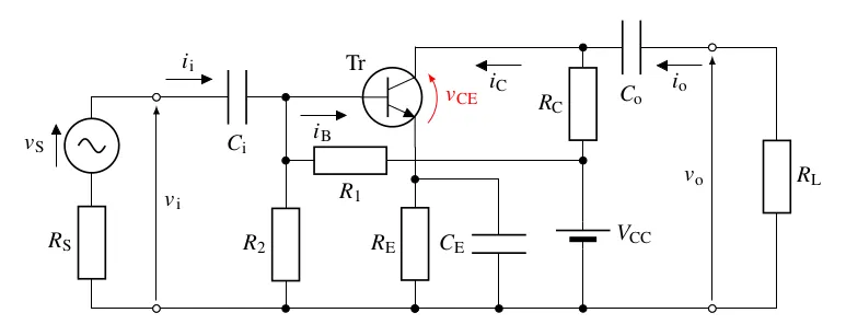
下図に示す電流帰還バイアス増幅回路で結合コンデンサ 、 が十分大きいとき、電圧増幅度 を簡易等価回路によって求めます。
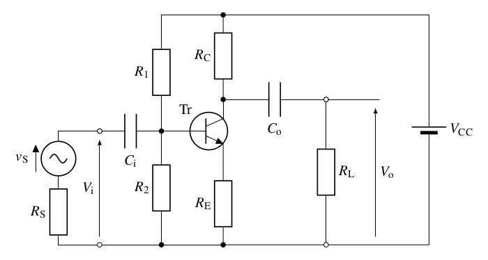
まずは下図に示すように簡易等価回路を描きます。 エミッタ抵抗 を描き忘れないように注意が必要です。
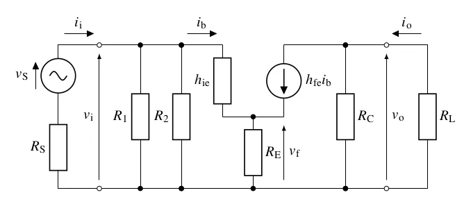
結合コンデンサの効果で 、 となるので、 となります。
と の並列合成抵抗を とおくと、入力電圧 、出力電圧 はそれぞれ以下の式で表されます。
したがって、電圧増幅度 は以下の式で与えられます。
、 より、上式は近似的に となります。 特に ならば となるので、その場合は となります。
したがって、この回路は の個体差を気にすることなく、抵抗の比だけで電圧増幅度を設定できます。
ただし、抵抗の設定次第でどこまでも電圧増幅度を高めることができるというわけではありません。
なので はほぼそのまま と の電圧降下の比となりますが、 を大きくするほどコレクタ-エミッタ間電圧が低下し、電流を十分流すことのできない飽和領域に接近します。 そのため、この回路は固定バイアス増幅回路ほど高い電圧増幅度が出せません。
バイパスコンデンサ挿入時の交流動作
電流帰還バイアス回路の安定性を活かしつつより大きな利得を得るため、下図に示すように、エミッタ抵抗に並列にコンデンサが挿入されることがしばしばあります1。 図の のように、交流信号のみをグランドに退避させるためのコンデンサをバイパスコンデンサ(側路コンデンサ)といいます。
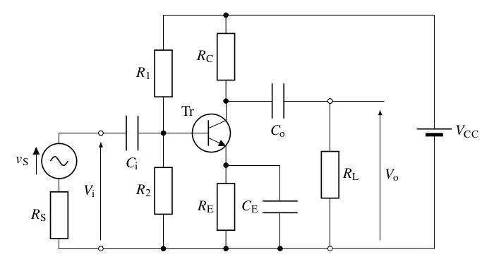
では、上図のようにバイパスコンデンサ を挿入した場合の電圧増幅度 を求めます。
簡易等価回路は下図のようになります。
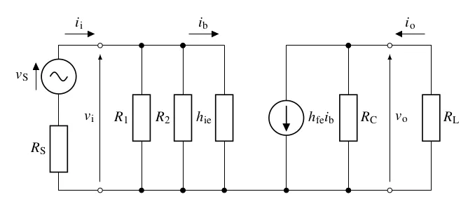
先ほどと同様に 、 となるので、 です。
また、(これは偶然ですが)上の回路の と を並列合成抵抗 に置き換えれば、前回の記事の練習問題3で扱った固定バイアス増幅回路の簡易等価回路と一致するので、その結果から電圧増幅度が以下の式で与えられます。
上式はベースに を接続した固定バイアス増幅回路の電圧増幅度 と一致します。
このように、 が十分大きい場合2においては、固定バイアス増幅回路と同様にトランジスタの に応じて目一杯の利得を出すことができます。
負帰還増幅回路
本記事の最初に取り上げた のない電流帰還バイアス増幅回路は、出力の一部を入力に戻す負帰還増幅回路です。
原理
まずは一般的な負帰還増幅回路の原理について、下のブロック線図3を用いて説明します。
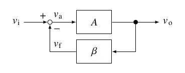
負帰還増幅回路は一般に、入力の 倍の電圧 を出力する増幅回路(図の )と、その出力を 倍した電圧 を増幅回路の入力側に戻す帰還回路(図の )で構成されます。
ブロック線図の加え合わせ点を見ると、入力電圧 と帰還電圧 は異符号となっています。 これは を と逆相で戻すことを意味しています。 このように、出力電圧の一部を入力信号と逆相で帰還することを負帰還といいます。
ブロック線図から、この負帰還増幅回路の全体の電圧増幅度 の公式が導出できます。
倍の増幅回路のみの場合に比べ、負帰還増幅回路の利得は 分の1に低下します。 このように利得は低下するものの、回路の安定性を向上させ、より広帯域にわたって一定の増幅度を実現することができます(詳細は割愛)。
用語
負帰還増幅回路に関する用語を表にまとめました。
| 用語 | 記号 | 意味 |
|---|---|---|
| 負帰還 | 入力電圧と逆相の電圧を帰還すること(対義語は正帰還) | |
| 帰還電圧 | 出力電圧に比例し、入力側に帰還される電圧 | |
| 開ループ利得 | 帰還機能のない増幅回路単体の電圧増幅度 | |
| 帰還率 | 出力電圧に対する帰還電圧の割合 | |
| 閉ループ利得 | 負帰還増幅回路全体の電圧増幅度 | |
| ループ利得 | 増幅回路と帰還回路からなるループを一周した電圧増幅度 |
ややこしいですが、ループ利得は開ループ利得や閉ループ利得とは別物です。
電流帰還バイアス増幅回路の場合
冒頭で電圧増幅度を計算した のない電流帰還バイアス増幅回路について、負帰還増幅回路の観点から説明します。 まずは帰還の仕組みを説明します。
帰還の仕組み
簡易等価回路を再掲します。
この回路の帰還の仕組みは、本質的には過去の記事で説明した直流動作と同様です。 簡易等価回路で説明すると、トランジスタの出力電流であるコレクタ電流 が増加すると、コレクタ電流とほぼ等しいエミッタ電流が増加し、それに応じて での電圧降下が増大し、トランジスタの入力電圧であるベース-エミッタ間電圧 を下げます。 これにより が低下し、コレクタ電流 が下がる、という流れです。
このように、この回路の負帰還の強さは の電圧降下で決まるので、 が短絡されている場合は負帰還増幅回路ではなくなります。 が交流的に短絡されている場合、 での電圧降下は直流成分のみとなるため、直流動作としてバイアス点を安定させるための負帰還は働きますが、交流信号の増幅動作の観点では帰還が働くことはありません。 したがって、 が挿入された電流帰還バイアス増幅回路は負帰還増幅回路ではありません。
開ループ利得と帰還率
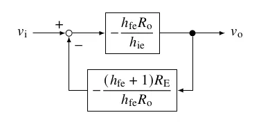
以上の説明や上図の簡易等価回路をブロック線図と対応付けると、「 での電圧降下」は帰還電圧 に、「ベース-エミッタ間電圧」は入力電圧と帰還電圧の差、すなわち で与えられるため にあたります。
挿入時は帰還が起こらないので、開ループ利得 は次式で表される 挿入時の電圧増幅度となります。
また、、 より、帰還率 は次式で表されます。
なので、帰還率は となります。 さらに、 ならば となります。
なお、 の負号は と が逆相であることを、 の負号は と が逆相であることを示しています。
ブロック線図による表現
上述した や を踏まえ、本記事の冒頭で計算した電圧増幅度 の式を以下のように変形すると、一般的な負帰還増幅回路の閉ループ利得の公式に帰着します。
したがって、 を挿入しない電流帰還バイアス増幅回路は、負帰還増幅回路として以下のブロック線図で表されます。
練習問題
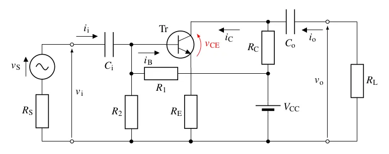
下図のトランジスタ回路において、以下の問いに答えよ。
(1) 電流増幅度 、 および入力インピーダンス を求めよ。ただし、、 とし、回答には を用いてもよい。
(2) いま、 に並列にコンデンサ を接続する。 が十分大きいとき、、、 を求めよ。
解説
この回路は電流帰還バイアス増幅回路を書き換えたものです。
(1) 問題文のとおりに をおくと、簡易等価回路は以下のように表されます。
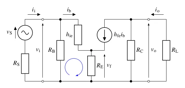
より、出力電流 は以下の式で表されます。
したがって、電流増幅度 は以下の式で与えられます。
上図の青矢印で示した閉路にキルヒホッフの電圧則を適用すると、以下のように が求められます。
したがって、電流増幅度 は 、 を用いて次式で表されます。
より、入力インピーダンス は を用いて次式で表されます。
(2) 下図のように を挿入したとき、簡易等価回路は上図で を短絡したものとなります。
したがって、上述の計算結果に を代入することで、 挿入時の電流増幅度や入力インピーダンスが求められ、その結果は以下のようになります。
※ 電圧増幅度だけでなく、電流増幅度や入力インピーダンスも前回の記事の練習問題3で扱った固定バイアス増幅回路における式と一致します。
おわりに
今回はトランジスタの パラメータによる簡易等価回路を用いて、電流帰還バイアス増幅回路の交流動作を解析しました。
バイパスコンデンサの挿入時と非挿入時の動作の違い、負帰還増幅回路の原理を具体例と関連付けて理解しました。
トランジスタ1個で構成され、「エミッタ接地増幅回路」と称して書籍などに載っている回路はたいてい固定バイアス増幅回路か電流帰還バイアス増幅回路ですが、今回の記事をもって、いずれの回路の直流動作も交流動作もまとめることができました。
直感的な動作原理とその数式的な表現を結び付けて理解することができたので、電子回路、特にトランジスタ回路を学んでいくための基礎固めができたのではないかと思います。
「学習帳」カテゴリの電子回路の記事はバイアス回路に始まり、4回連続でトランジスタ回路を扱ってきました。 今後は回路シミュレータや発振回路についても学びたいところなのですが、増幅回路の基礎理論としてはひとまずこの記事で区切りがつきました。 また気が向いたら学習に取り組もうと思います。
回路図のソースコード
回路図は を用いて で作成しています。 ソースコードは以下のとおりです。
電流帰還バイアス増幅回路 (voltage-divider-bias-amp-1.tex)
% Common Emitter Amplifier (voltage divider bias)
\documentclass[border=3mm]{standalone}
\usepackage{tikz}
\usepackage{circuitikz}
\usetikzlibrary{calc}
\ctikzset{transistors/arrow pos=end}
\usepackage{newtxtext,newtxmath}
\pagecolor{white}
\begin{document}
\begin{tikzpicture}
\draw (0,0) node[npn](Tr) {};
\draw[thick] ($(Tr)-(0.35,0)$) circle [radius=13pt] node[above left=8pt] {Tr};
\draw(Tr.E)
    to[european resistor, l_=$R_\mathrm{E}$] ++(0,-2)
    coordinate(tmp3) % below Re
    to[short] ++(2.5,0)
    coordinate(tmp6) % below Rl
    to[short] ++(2.5,0)
    to[battery2, invert, l_=$V_\mathrm{CC}$] ++(0,5.6)
    to[short] ++(-5,0)
    coordinate(tmp1) % above Rc
    to[european resistor, l_=$R_\mathrm{C}$] ++(0,-2)
    to[short] (Tr.C);
\draw(tmp1)
    to[short, *-] ++(-1.5,0)
    to[european resistor, l_=$R_1$] ++(0,-2.8) |- (Tr.B)
    node[pos=0.5, coordinate] (tmp5) {};
\draw(tmp5) to[short, *-] (Tr.B);
\draw(tmp3)
    to[short, *-] ++(-1.5,0)
    to[european resistor=$R_2$, *-] (tmp5);
\draw(Tr.C)
    to[C, l_=$C_\mathrm{o}$, *-] ++(2.5,0)
    coordinate(tmp7)
    to[european resistor, l=$R_\mathrm{L}$, o-o] (tmp6);
\draw(tmp5)
    to[C, l=$C_\mathrm{i}$, -o] ++(-1.5,0)
    coordinate(tmp8);
\draw(tmp3)
    to[short] ++(-3,0)
    coordinate(tmp9)
    to[short, o-] ++(-1,0)
    to[european resistor, l=$R_\mathrm{S}$] ++(0,1.6)
    to[sV=$v_\mathrm{S}$] ++(0,1) |- (tmp8) to[short, -o] (tmp8);
\draw(tmp7) to[short, o-] ++(1.3,0);
\draw[-latex] ($(tmp6)+(1.2,0.2)$) -- ($(tmp7)+(1.2,-0.2)$)
    node[pos=0.5, right] {$V_\mathrm{o}$};
\draw[-latex] ($(tmp9)+(0,0.2)$) -- ($(tmp8)+(0,-0.2)$)
    node[pos=0.5, left] {$V_\mathrm{i}$};
%%% [BEGIN] Bypass capacitor %%%
\draw(Tr.E)
    to[short, *-] ++(1.3,0)
    to[C, l_=$C_\mathrm{E}$, -*] ++(0,-2);
%%%  [END]  Bypass capacitor %%%
\end{tikzpicture}
\end{document}
簡易等価回路(バイパスコンデンサなし) (simple-equiv-circuit.tex)
% Simple Equivalent Circuit (w/o Ce)
\documentclass[border=3mm]{standalone}
\usepackage{tikz}
\usepackage{circuitikz}
\usepackage{newtxtext,newtxmath}
\pagecolor{white}
\begin{document}
\begin{tikzpicture}
%%% [BEGIN] equivalent circuit of common emitter BJT %%%
\draw (0,0) to[european resistor, l_=$h_\mathrm{ie}$] ++(0,-1.75);
\draw (1.5,0) to[american current source, l=$h_\mathrm{fe}i_\mathrm{b}$] ++(0,-1.75);
\draw (0,0) to[short, f<_=$i_\mathrm{b}$, -o] ++(-1,0);
\draw (1.5,0) to[short, -o] ++(1.5,0);
\draw (-1,-3.5) to[short, o-o] (3,-3.5);
\draw (0,-1.75) to[short] ++(1.5,0);
%%%  [END]  equivalent circuit of common emitter BJT %%%
\draw (0.75,-1.75) to[european resistor, l=$R_\mathrm{E}$, *-*] ++(0,-1.75);
\draw[-latex] (1.5,-3.3) -- (1.5,-1.95) node[pos=0.5, right] {$v_\mathrm{f}$};
%%% [BEGIN] input %%%
\draw (-2,0) to[european resistor, l_=$R_1$, *-*] ++(0,-3.5);
\draw (-1,0) to[european resistor, l_=$R_2$, *-*] ++(0,-3.5);
\draw (-1,0) to[short, -o] ++(-2,0) to[short, f<_=$i_\mathrm{i}$] ++(-1,0)
    to[sV_<=$v_\mathrm{S}$] ++(0,-1.5)
    to[european resistor, l_=$R_\mathrm{S}$] ++(0,-2)
    to[short] ++(1,0) to[short, o-] ++(2,0);
\draw[-latex] (-3,-3.3) -- (-3,-0.2) node[pos=0.5, left] {$v_\mathrm{i}$};
%%%  [END]  input %%%
%%% [BEGIN] output %%%
\draw (3,0) to[european resistor, l=$R_\mathrm{C}$, *-*] ++(0,-3.5);
\draw (3,0) to[short, -o] ++(1,0) to[short, f<=$i_\mathrm{o}$] ++(1,0)
    to[european resistor, l=$R_\mathrm{L}$] ++(0,-3.5) to[short] ++(-1,0)
    to[short, o-] ++(-1,0);
\draw[-latex] (4,-3.3) -- (4,-0.2) node[pos=0.5, right] {$v_\mathrm{o}$};
%%%  [END]  output %%%
\end{tikzpicture}
\end{document}
簡易等価回路(バイパスコンデンサあり) (simple-equiv-circuit-with-bypass-capacitor.tex)
% Simple Equivalent Circuit (w/ Ce)
\documentclass[border=3mm]{standalone}
\usepackage{tikz}
\usepackage{circuitikz}
\usepackage{newtxtext,newtxmath}
\pagecolor{white}
\begin{document}
\begin{tikzpicture}
%%% [BEGIN] equivalent circuit of common emitter BJT %%%
\draw (0,0) to[european resistor, l_=$h_\mathrm{ie}$, -*] ++(0,-3.5);
\draw (1.5,0) to[american current source, l=$h_\mathrm{fe}i_\mathrm{b}$, -*] ++(0,-3.5);
\draw (0,0) to[short, f<_=$i_\mathrm{b}$, -o] ++(-1,0);
\draw (1.5,0) to[short, -o] ++(1.5,0);
\draw (-1,-3.5) to[short, o-o] (3,-3.5);
%%%  [END]  equivalent circuit of common emitter BJT %%%
%%% [BEGIN] input %%%
\draw (-2,0) to[european resistor, l_=$R_1$, *-*] ++(0,-3.5);
\draw (-1,0) to[european resistor, l_=$R_2$, *-*] ++(0,-3.5);
\draw (-1,0) to[short, -o] ++(-2,0) to[short, f<_=$i_\mathrm{i}$] ++(-1,0)
    to[sV_<=$v_\mathrm{S}$] ++(0,-1.5)
    to[european resistor, l_=$R_\mathrm{S}$] ++(0,-2)
    to[short] ++(1,0) to[short, o-] ++(2,0);
\draw[-latex] (-3,-3.3) -- (-3,-0.2) node[pos=0.5, left] {$v_\mathrm{i}$};
%%%  [END]  input %%%
%%% [BEGIN] output %%%
\draw (3,0) to[european resistor, l=$R_\mathrm{C}$, *-*] ++(0,-3.5);
\draw (3,0) to[short, -o] ++(1,0) to[short, f<=$i_\mathrm{o}$] ++(1,0)
    to[european resistor, l=$R_\mathrm{L}$] ++(0,-3.5) to[short] ++(-1,0)
    to[short, o-] ++(-1,0);
\draw[-latex] (4,-3.3) -- (4,-0.2) node[pos=0.5, right] {$v_\mathrm{o}$};
%%%  [END]  output %%%
\end{tikzpicture}
\end{document}
電流帰還バイアス増幅回路(練習問題) (voltage-divider-bias-amp-2.tex)
% Voltage Divider Bias Circuit
\documentclass[border=3mm]{standalone}
\usepackage{tikz}
\usepackage{circuitikz}
\ctikzset{transistors/arrow pos=end}
\usepackage{newtxtext,newtxmath}
\pagecolor{white}
\begin{document}
\begin{tikzpicture}
\draw (0,0) node[npn](Tr) {};
\draw[thick] ($(Tr)-(0.35,0)$) circle [radius=13pt] node[above left=8pt] {Tr};
\draw[red, -latex] (0.2,-0.4) arc[x radius=0.6, y radius=0.6, start angle=320, delta angle=80]
    node[below right=4pt] {$v_\mathrm{CE}$};
\draw(Tr.C)
    to[short, f<_=$i_\mathrm{C}$] ++(2.6,0)
    to[european resistor, l_=$R_\mathrm{C}$] ++(0,-1.75)
    coordinate(tmp0) % below Rc
    to[short] ++(-2.6,0)
    to[european resistor, l=$R_1$] ++(-2,0)
    coordinate(tmp1) % left R1
    to[short] ++(0,0.95) |- (Tr.B)
    node[pos=0.5, circ] (tmp3) {}; % ;
\draw(tmp3) to[short, f_=$i_\mathrm{B}$] (Tr.B);
\draw(Tr.E)
    to[short] ++(0,-0.5)
    to[european resistor, l_=$R_\mathrm{E}$, -*] ++(0,-2)
    coordinate(tmp2); % below Re
\draw(tmp0)
    to[battery2, l=$V_\mathrm{CC}$, *-] ++(0,-2.3) |- (tmp2);
\draw(tmp1)
    to[short, *-] ++(0,-0.3)
    to[european resistor, l_=$R_2$] ++(0,-2) |- (tmp2)
    node[pos=0.5, circ] {};
%%% [BEGIN] Bypass capacitor %%%
\draw(Tr.E)
    to[short] ++(0,-0.5)
    to[short, *-] ++(1.3,0)
    to[C, l_=$C_\mathrm{E}$, -*] ++(0,-2);
%%%  [END]  Bypass capacitor %%%
%%% [BEGIN] I/O %%%
% --- Input ---
\draw(tmp3)
    to[short] ++(-0.5,0) to[C, l=$C_\mathrm{i}$] ++(-0.5,0)
    to[short, f_<=$i_\mathrm{i}$, -o] ++(-1,0) node (inp) {};
\draw(tmp2) to[short, *-o] ++(-4,0) node (inn) {};
\draw[-latex] (inn) -- (inp) node[right,pos=0.5] {$v_\mathrm{i}$};
% --- Output ---
\draw(Tr.C) to[short, -*] ++(2.6,0)
    to[short] ++(0.5,0) to[C, l_=$C_\mathrm{o}$] ++(0.5,0)
    to[short, f_<=$i_\mathrm{o}$, -o] ++(1,0) node (outp) {};
\draw(tmp2) to[short, -*] ++(2.6,0)
    to[short, -o] ++(2,0) node (outn) {};
\draw[-latex] (outn) -- (outp) node[left,pos=0.5] {$v_\mathrm{o}$};
%%%  [END]  I/O %%%
%%% [BEGIN] Load & Source %%%
\draw(outp.center) to[short, o-] ++(1,0)
    to[european resistor, l=$R_\mathrm{L}$] ++(0,-4) |- (outn.center)
    node[pos=0.5] {} to[short, -o] (outn.center);
\draw(inp.center) to[short, o-] ++(-1,0)
    to[sV_<=$v_\mathrm{S}$] ++(0,-1.5)
    to[european resistor, l_=$R_\mathrm{S}$] ++(0,-1.5) |- (inn.center)
    node[pos=0.5] {} to[short, -o] (inn.center);
%%%  [END]  Load & Source %%%
\end{tikzpicture}
\end{document}
簡易等価回路(練習問題の解説) (practice-equiv-circuit.tex)
% Simple Equivalent Circuit (w/o Ce)
\documentclass[border=3mm]{standalone}
\usepackage{tikz}
\usepackage{circuitikz}
\usepackage{newtxtext,newtxmath}
\pagecolor{white}
\begin{document}
\begin{tikzpicture}
%%% [BEGIN] equivalent circuit of common emitter BJT %%%
\draw (0,0) to[european resistor, l_=$h_\mathrm{ie}$] ++(0,-1.75);
\draw (1.5,0) to[american current source, l=$h_\mathrm{fe}i_\mathrm{b}$] ++(0,-1.75);
\draw (0,0) to[short, f<_=$i_\mathrm{b}$, -o] ++(-1,0);
\draw (1.5,0) to[short, -o] ++(1.5,0);
\draw (-1,-3.5) to[short, o-o] (3,-3.5);
\draw (0,-1.75) to[short] ++(1.5,0);
\draw (0.75,-1.75) to[european resistor, l=$R_\mathrm{E}$, *-*] ++(0,-1.75);
\draw[-latex] (1.5,-3.3) -- (1.5,-1.95) node[pos=0.5, right] {$v_\mathrm{f}$};
%%%  [END]  equivalent circuit of common emitter BJT %%%
%%% [BEGIN] input %%%
\draw (-1,0) to[european resistor, l_=$R_\mathrm{B}$, *-*] ++(0,-3.5);
\draw (-1,0) to[short, -o] ++(-1,0) to[short, f<_=$i_\mathrm{i}$] ++(-1,0)
    to[sV_<=$v_\mathrm{S}$] ++(0,-1.5)
    to[european resistor, l_=$R_\mathrm{S}$] ++(0,-2)
    to[short] ++(1,0) to[short, o-] ++(1,0);
\draw[-latex] (-2,-3.3) -- (-2,-0.2) node[pos=0.5, left] {$v_\mathrm{i}$};
%%%  [END]  input %%%
%%% [BEGIN] output %%%
\draw (3,0) to[european resistor, l=$R_\mathrm{C}$, *-*] ++(0,-3.5);
\draw (3,0) to[short, -o] ++(1,0) to[short, f<=$i_\mathrm{o}$] ++(1,0)
    to[european resistor, l=$R_\mathrm{L}$] ++(0,-3.5) to[short] ++(-1,0)
    to[short, o-] ++(-1,0);
\draw[-latex] (4,-3.3) -- (4,-0.2) node[pos=0.5, right] {$v_\mathrm{o}$};
%%%  [END]  output %%%
%%% [BEGIN] loop %%%
\draw[blue, latex-] (-0.15,-3.2) arc[x radius=0.5, y radius=0.5, start angle=280, delta angle=320];
%%%  [END]  loop %%%
\end{tikzpicture}
\end{document}
その他図面のソースコード
回路図以外の図も を用いて で作成しています。 ソースコードは以下のとおりです。
負帰還増幅回路の原理図 (negative-feedback.tex)
% Block Diagram of Negative Feedback Amplifier
\documentclass[border=3mm]{standalone}
\usepackage{tikz}
\usepackage{circuitikz}
\usetikzlibrary{positioning}
\usepackage{newtxtext,newtxmath}
\pagecolor{white}
\begin{document}
\begin{tikzpicture}[>=latex,
    block/.style={draw, rectangle, minimum width=1.2cm, minimum height=0.8cm, align=center},
    sum/.style={draw, circle, minimum size=1.5mm, inner sep=0pt}]
    \node[block] (A) at (1.5, 1.4) {$A$};
    \node[block] (beta) at (1.5, 0.4) {$\beta$};
    \node[sum, left=0.8cm of A] (sum) {};
    \node[left=0.8cm of sum] (Vi) {$v_\mathrm{i}$};
    \node[right=1.6cm of A] (Vo) {$v_\mathrm{o}$};
    \draw[->] (Vi) -- (sum) node[pos=0.8, above] {$+$};
    \draw[<-] (A) -- (sum) node[above right] {$v_\mathrm{a}$};
    \draw[->] (A) -- (Vo)
        node[pos=0.5, circle, fill=black, minimum size=1.5mm, inner sep=0pt, outer sep=0pt] (branch) {};
    \draw[->] (branch) |- (beta);
    \draw[->] (beta) -| (sum) node[pos=0.9, right] {$-$} node[pos=0.5, above right] {$v_\mathrm{f}$};
\end{tikzpicture}
\end{document}
電流帰還バイアス回路のブロック線図 (blk-diag-voltage-divider.tex)
% Block Diagram of Voltage Divider Bias Amplifier
\documentclass[border=3mm]{standalone}
\usepackage{tikz}
\usepackage{circuitikz}
\usetikzlibrary{positioning}
\usepackage{newtxtext,newtxmath}
\pagecolor{white}
\begin{document}
\begin{tikzpicture}[>=latex,
    block/.style={draw, rectangle, minimum width=1.2cm, minimum height=0.8cm, align=center},
    sum/.style={draw, circle, minimum size=1.5mm, inner sep=0pt}]
    \node[block] (A) at (1.5, 1.4) {$-\dfrac{h_\mathrm{fe}R_\mathrm{o}}{h_\mathrm{ie}}$};
    \node[block] (beta) at (1.5, 0) {$-\dfrac{(h_\mathrm{fe}+1)R_\mathrm{E}}{h_\mathrm{fe}R_\mathrm{o}}$};
    \node[sum, left=0.8cm of A] (sum) {};
    \node[left=0.8cm of sum] (Vi) {$v_\mathrm{i}$};
    \node[right=1.6cm of A] (Vo) {$v_\mathrm{o}$};
    \draw[->] (Vi) -- (sum) node[pos=0.8, above] {$+$};
    \draw[<-] (A) -- (sum); % node[above right] {$v_\mathrm{a}$};
    \draw[->] (A) -- (Vo)
        node[pos=0.5, circle, fill=black, minimum size=1.5mm, inner sep=0pt, outer sep=0pt] (branch) {};
    \draw[->] (branch) |- (beta);
    \draw[->] (beta) -| (sum) node[pos=0.9, right] {$-$}; % node[pos=0.5, above right] {$v_\mathrm{f}$};
\end{tikzpicture}
\end{document}