はじめに
前回の記事では、バイポーラトランジスタ(以下「トランジスタ」)のバイアス回路の直流動作を計算によって解析しました。 この計算ではベース-エミッタ間電圧 やエミッタ接地直流電流増幅率 を一定とおいて簡単化していました。
しかし、実際は はベース電流 によって変化するうえ、 は温度だけでなく、コレクタ電流 によっても変化します。 さらに、 はコレクタ-エミッタ間電圧 によっても変動します。
そこで今回は、トランジスタのエミッタ接地における入力特性と出力特性のグラフを通して、計算で考慮していなかったトランジスタの実際の特性を理解します。
また、バイアス回路を例に負荷線と動作点を用いたトランジスタ回路の解析手法に触れ、回路の安定性を比較します。
トランジスタの入出力特性
入力特性
エミッタ接地回路ではトランジスタのベース-エミッタ間を入力端として利用することから、 特性、つまり、ベース-エミッタ間の電流-電圧特性を入力特性と呼んでいます。
ベース-エミッタ間はpn接合で構成されているため、入力特性は理論的にはショックレーの式によって与えられ、電流は電圧に対して(比例関係ではなく)指数関数的に増加します。
下図の実線はショックレーの式を適当なパラメータを入れてプロットしたものです1。 付近で電流が急上昇していることが分かります。
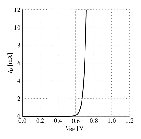
前回の記事で行ったバイアス回路の計算では、 一定としていました。 これは上図の破線に対応します。
上図より、 が大きい領域だけでなく、 が小さい領域でも 0.6 V 一定とする近似との乖離が大きくなっていくことが分かります。
仮に上図の入力特性を有するトランジスタを使った場合、 が から 程度ならば 0.6 V は妥当な近似ですが、 ならば なので、0.5 V の方が近似誤差は少なくなります。
出力特性
エミッタ接地回路ではトランジスタのコレクタ-エミッタ間を出力端として利用することから、 特性、つまり、コレクタ-エミッタ間の電流-電圧特性を出力特性と呼んでいます。
前回の記事で行った回路計算では かつ は一定(例えば )としていました。 この仮定通りに動作するなら、出力特性は下図のようになるはずです。
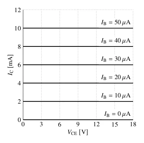
上図の特徴は、横軸に平行な直線が等間隔に並んでいることです。 これは、 が によらない の定数倍となる(その定数こそが )という、電流源としても増幅素子としても理想的な出力特性を示しています。
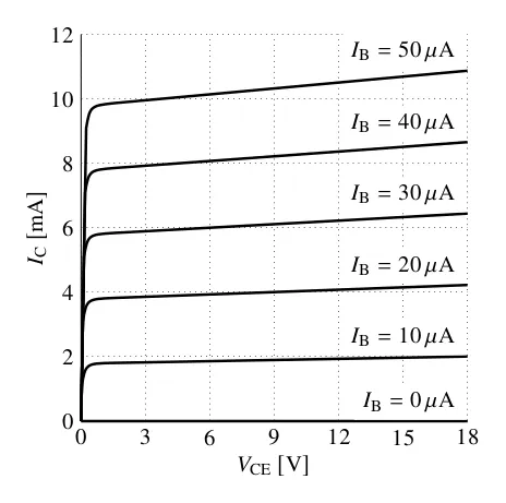
しかし、データシートで見るような出力特性は下図のように複雑な形状をしています。
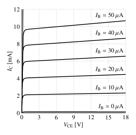
2つの出力特性の図を比較すると、以下の3つの違いがあります。
1. 飽和領域と遮断領域の存在
トランジスタの出力特性は活性領域、飽和領域(図の左側の灰色部分)、遮断領域(図の下側の灰色部分)の3つに分けられます。 3つの領域の特徴を下表に示します。
| 領域 | ベース-エミッタ間 | ベース-コレクタ間 | 特徴 |
|---|---|---|---|
| 活性領域 | 順方向バイアス | 逆方向バイアス | 増幅回路で利用する領域 |
| 飽和領域 | 順方向バイアス | 順方向バイアス | が 0 V に近く が十分流せなくなる |
| 遮断領域 | 逆方向バイアス | 逆方向バイアス | が加えられていても はほとんど流れない2 |
前回の記事で行った回路計算では活性領域のみを考慮しており、飽和領域と遮断領域は暗黙的に無視していました。 実際は計算式とは異なり、 となっても が流れるわけではなく、 でも が(微小ながら)流れているということです。
また、活性領域の中でも理想的な出力特性との違いが見て取れます。 続く2と3で説明します。
2. 直流電流増幅率のコレクタ電流依存性
の活性領域を見ると、 と の曲線の間隔に比べ、 と の曲線の間隔が狭くなっていることが分かります。
曲線の間隔が等間隔でないとは、すなわち が に依存するということです。 これは、回路計算でよく使う の式における が に依存するため、比例「定数」ではないことを意味するものです。
実はトランジスタのデータシートには 特性曲線も掲載されていて、 が一定のとき、 がある程度まで増加すると が急激に低下する様子が描かれています。
これについてGeminiに訊いたところ、 が大きくなるとコレクタのキャリアが大量にベースに押し寄せ、実効的なベース幅が広がることが原因とのことです。
3. コレクタ電流のコレクタ電圧依存性
活性領域で目を引くのが、曲線が斜め上を向いていることと、その仰角が によって異なることです。
曲線が傾いているということは、つまり が によらず一定とはならないことです。
トランジスタにおいて が増大すると も増大するこの現象はアーリー効果と呼ばれています。
アーリー効果は が大きくなるとベース-コレクタ間の空乏層が増大し、実効的なベース幅が狭まることが原因で生じるそうです。
バイアス回路の図式解析
ここからはトランジスタの特性曲線を利用してトランジスタ回路の直流動作を見ていきます。
具体的には、出力特性のグラフ上に回路ごとに決まる負荷線を引き、その線上に回路の動作点を作図することにより、回路がどの領域のどこで動作しているのかを調べます。
回路
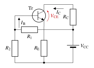
ここでは前回最初に扱った下図の固定バイアス回路を考えます3。
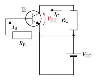
ここで、、 とし、回路で使用するトランジスタは下図に示す出力特性を有するものとします。 また、ベース電流は とします。
以下では上図の出力特性のグラフに負荷線と動作点を作図します。
負荷線
まずは負荷線を作図します。 は回路図より次式で表されます。
は に関する一次関数のため、負荷線は直線となることが分かります。
また、、 より、負荷線は と の2点を通る直線であることが分かります。 この2点の座標から負荷線が作図できます(下図の赤い直線)。
この固定バイアス回路は出力特性のグラフの中でも、この負荷線上のある点で動作します。 この点を動作点と呼びます。
動作点
動作点は特性曲線と負荷線の交点です。
したがって、 のときの動作点は出力特性曲線と負荷線の交点である下図の点Pです。
点Pを見れば、動作点Pにおけるコレクタ-エミッタ間電圧とコレクタ電流がそれぞれ 、 であることが読み取れます。
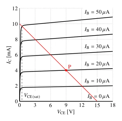
さて、上図の負荷線と出力特性曲線を見ると、 が 0.5 V ほどまで低下すると電流が飽和し、 がそれより下がらなくなることが読み取れます。 このときの の値をコレクタ-エミッタ間遮断電圧 と呼びます(上図参照)。 トランジスタのデータシートには 特性も載っています。
練習問題
下図の回路におけるトランジスタの出力特性と回路の負荷線が上図で表されるとき、コレクタ抵抗 を求めよ。 ただし、エミッタ抵抗 であり、回路は点Pで動作しているものとし、エミッタ電流 は とする。
バイアス点の安定性
バイアス回路の安定性については前回の記事でも評価しましたが、今回は出力特性のグラフを用いて考察します。
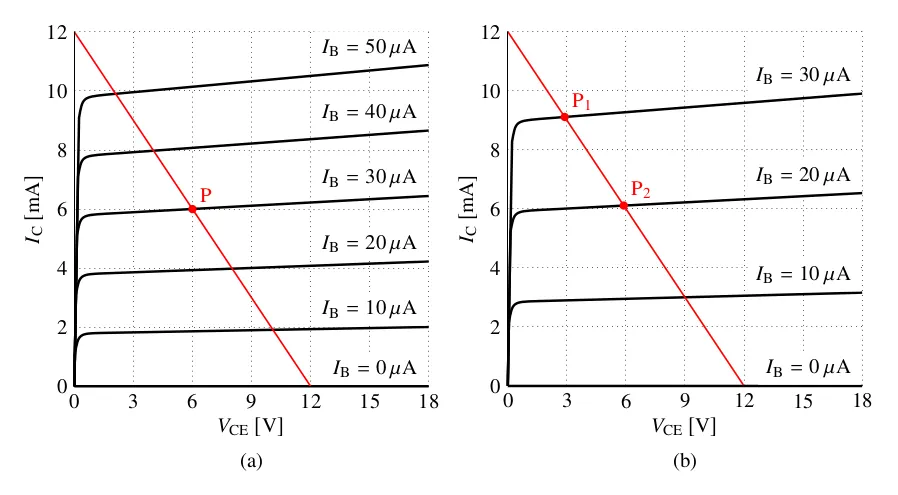
負荷線と動作点Pがいずれも上図(a)で表される固定バイアス回路と電流帰還バイアス回路を考えます。
が約1.5倍に増加すると、特性曲線は上図(b)のように縦に拡大します。 このとき、図(a)の点Pの位置にあった各バイアス回路の動作点(バイアス点)が移動しますが、その移動距離は両者で大きく異なります。
固定バイアス回路の場合は が固定されているので、動作点も出力特性の曲線に合わせて上方に動きます。 簡単のため の変動を無視すると、 はそのまま、動作点は図(b)の の位置に動きます。
電流帰還バイアス回路は がエミッタ抵抗によって強力に固定されているので、出力特性曲線が全体的に上にシフトしても、動作点は負荷線と の水平線との交点をほとんど動きません。 その代わりに は自動的に低下するため、動作点を通る特性曲線が変わります。 例えば をほぼ一定に保った結果 となった場合、動作点は図(b)の の位置に動きます。
電流帰還バイアス回路は固定バイアス回路に比べてほとんど動作点が動きません。 このように図で見るとその安定性は一目瞭然です。
おわりに
本記事では入力特性と出力特性を通してトランジスタの動作への理解を深め、バイアス回路の動作や安定性を読み解きました。
現実のトランジスタの動作は様々な仮定をおいた回路計算のように単純ではありませんが、それらの仮定が妥当といえる範囲内で動作させる限り、概ね計算通りの傾向が得られます。
さて、今回は直流と交流で同じ負荷線となる回路を取り上げましたが、一般には直流と交流で負荷線が異なります。 その場合は直流負荷線で動作点を求め、交流動作は交流負荷線上で解析することになります。
直流動作と分けて考える交流動作については、機会があれば取り上げたいと思います(2026/06/21追記:続編の記事で取り上げました)。
回路図のソースコード
回路図は を用いて で作成しています。 ソースコードは以下のとおりです。
固定バイアス回路 (fixed2.tex)
% Fixed Bias Circuit (2)
\documentclass[border=3mm]{standalone}
\usepackage{tikz}
\usepackage{circuitikz}
\ctikzset{transistors/arrow pos=end}
\usepackage{newtxtext,newtxmath}
\pagecolor{white}
\begin{document}
\begin{tikzpicture}
\draw (0,0) node[npn](Tr) {};
\draw[thick] ($(Tr)-(0.35,0)$) circle [radius=13pt] node[above left=8pt] {Tr};
\draw[red, -latex] (0.2,-0.4) arc[x radius=0.6, y radius=0.6, start angle=320, delta angle=80]
    node[below right=4pt] {$V_\mathrm{CE}$};
\draw(Tr.C)
    to[short, f<_=$I_\mathrm{C}$] ++(2,0)
    to[european resistor, l_=$R_\mathrm{C}$] ++(0,-1.75)
    coordinate(tmp0) % below Rc
    to[short] ++(-2,0)
    to[european resistor, l=$R_\mathrm{B}$] ++(-2,0)
    coordinate(tmp1) % left Rb
    to[short, f_=$I_\mathrm{B}$] ++(0,0.95) |- (Tr.B);
\draw(Tr.E)
    to[short] ++(0,-0.5)
    to[short] ++(0,-2)
    coordinate(tmp2); % below Tr.E
\draw(tmp0)
    to[battery2, l=$V_\mathrm{CC}$, *-] ++(0,-2.3) |- (tmp2);
\end{tikzpicture}
\end{document}
電流帰還バイアス回路 (voltage-divider2.tex)
% Voltage Divider Bias Circuit (2)
\documentclass[border=3mm]{standalone}
\usepackage{tikz}
\usepackage{circuitikz}
\ctikzset{transistors/arrow pos=end}
\usepackage{newtxtext,newtxmath}
\pagecolor{white}
\begin{document}
\begin{tikzpicture}
\draw (0,0) node[npn](Tr) {};
\draw[thick] ($(Tr)-(0.35,0)$) circle [radius=13pt] node[above left=8pt] {Tr};
\draw[red, -latex] (0.2,-0.4) arc[x radius=0.6, y radius=0.6, start angle=320, delta angle=80]
    node[below right=4pt] {$V_\mathrm{CE}$};
\draw(Tr.C)
    to[short, f<_=$I_\mathrm{C}$] ++(2,0)
    to[european resistor, l_=$R_\mathrm{C}$] ++(0,-1.75)
    coordinate(tmp0) % below Rc
    to[short] ++(-2,0)
    to[european resistor, l=$R_1$] ++(-2,0)
    coordinate(tmp1) % left R1
    to[short, f_=$I_\mathrm{B}$] ++(0,0.95) |- (Tr.B);
\draw(Tr.E)
    to[short] ++(0,-0.5)
    to[european resistor, l_=$R_\mathrm{E}$, -*] ++(0,-2)
    coordinate(tmp2); % below Re
\draw(tmp0)
    to[battery2, l=$V_\mathrm{CC}$, *-] ++(0,-2.3) |- (tmp2);
\draw(tmp1)
    to[short, *-] ++(0,-0.3)
    to[european resistor, l_=$R_2$] ++(0,-2) |- (tmp2);
\end{tikzpicture}
\end{document}
その他図面のソースコード
回路図以外の図も を用いて で作成しています。 ソースコードは以下のとおりです。
入力特性の例 (input.tex)
% Input Characteristics Curve
\documentclass[border=3mm]{standalone}
\usepackage{tikz}
\usetikzlibrary{intersections}
\usepackage{newtxtext,newtxmath}
\pagecolor{white}
\begin{document}
\begin{tikzpicture}
\draw[darkgray,dotted] (6,6) grid (0,0);
%%% [BEGIN] Characteristics curve %%%
% --- Theoretical --- % Is = 1e-14 A, T = 298.15 K
\draw[very thick] (0,0) -- (2.35,0) -- (2.4,0.001) -- (2.45,0.001)
    -- (2.5,0.001) -- (2.55,0.002) -- (2.6,0.003) -- (2.65,0.004)
    -- (2.7,0.007) -- (2.75,0.01) -- (2.8,0.014) -- (2.85,0.021)
    -- (2.9,0.031) -- (2.95,0.046) -- (3,0.067) -- (3.05,0.099)
    -- (3.1,0.146) -- (3.15,0.216) -- (3.2,0.318) -- (3.25,0.469)
    -- (3.3,0.692) -- (3.35,1.021) -- (3.4,1.506) -- (3.45,2.221)
    -- (3.5,3.276) -- (3.55,4.832) -- (3.5775,5.984);
% --- Approximated ---
\draw[thick,densely dashed] (3,0) -- (3,6);
%%%  [END]  Characteristics curve %%%
%%% [BEGIN] Axes %%%
\draw (0,0) -- (6,0) (0,0) -- (0,6);
\foreach \i in {0,1,...,6} {
    \pgfmathparse{\i*0.2}
    \let\x\pgfmathresult
    \node[below] at (\i,0) {\pgfmathprintnumber[fixed,fixed zerofill=true,precision=1]{\x}};
}
\foreach \i in {0,1,...,6} \node[left]  at (0,\i) {\the\numexpr\i*2\relax};
\node[below] at (3,-0.4) {$V_\mathrm{BE}\mathrm{\,[V]}$};
\node[rotate=90,above] at (-0.4,3) {$I_\mathrm{B}\mathrm{\,[mA]}$};
%%%  [END]  Axes %%%
\end{tikzpicture}
\end{document}
理想的な出力特性の例 (output-ideal.tex)
% Output Characteristics Curve (Ideal)
\documentclass[border=3mm]{standalone}
\usepackage{tikz}
\usetikzlibrary{intersections}
\usepackage{newtxtext,newtxmath}
\pagecolor{white}
\begin{document}
\begin{tikzpicture}
\draw[darkgray,dotted] (6,6) grid (0,0);
%%% [BEGIN] Ideal characteristics %%%
\foreach \i in {0,1,...,5}
    \draw[very thick] (0,\i) -- +(6,0)
        node[above left,fill=white] {$I_\mathrm{B}=\the\numexpr\i*10\relax\mathrm{\,\mu A}$};
%%%  [END]  Ideal characteristics %%%
%%% [BEGIN] Axes %%%
\draw (0,0) -- (6,0) (0,0) -- (0,6);
\foreach \i in {0,1,...,6} \node[below] at (\i,0) {\the\numexpr\i*3\relax};
\foreach \i in {0,1,...,6} \node[left]  at (0,\i) {\the\numexpr\i*2\relax};
\node[below] at (3,-0.4) {$V_\mathrm{CE}\mathrm{\,[V]}$};
\node[rotate=90,above] at (-0.4,3) {$I_\mathrm{C}\mathrm{\,[mA]}$};
%%%  [END]  Axes %%%
\end{tikzpicture}
\end{document}
出力特性の説明図 (output-sketch.tex)
% Output Characteristics Curve (Sketch)
\documentclass[border=3mm]{standalone}
\usepackage{tikz}
\usetikzlibrary{intersections}
\usepackage{newtxtext,newtxmath}
\pagecolor{white}
\begin{document}
\begin{tikzpicture}
\draw[darkgray,dotted] (6,6) grid (0,0);
%%% [BEGIN] Characteristics (sketch) %%%
\def\offset{-0.28}
\def\theta{89} % deg
\def\alpha{1} % deg
\def\beta{0.99}
% --- fill saturation region ---
\path[name path=lu] (0,6) -- (6,6);
\path[name path=lcut] (0,0) -- (\theta:6.2);
\path[name intersections={of=lu and lcut, name=pu}];
\fill[gray] (0,0) -- (pu-1) -- (0,6) -- cycle;
% --- draw curves ---
\path[name path=lr] (6,0) -- (6,6);
\foreach \i in {5,...,1} {
    \edef\curvepath{(\theta:{\offset+\i/sin(\theta)*\beta^\i}) .. controls +(80:0.35) .. ++({\alpha*\i+35}:0.6)}
    \path[name path=c] (0,0) -- \curvepath -- +({\alpha*\i}:5.5);
    \path[name intersections={of=lr and c, name=p}];
    \draw[very thick] (0,0) -- \curvepath -- (p-1)
        node[above left,fill=white] {$I_\mathrm{B}=\the\numexpr\i*10\relax\mathrm{\,\mu A}$};
}
% --- draw curve and fill cutoff region ---
    \edef\curvepath{(\theta:0) .. controls +(80:0.05) .. ++(20:0.2)}
    \path[name path=c] (0,0) -- \curvepath -- +(0:5.9);
    \path[name intersections={of=lr and c, name=p}];
    \fill[lightgray] (0,0) -- \curvepath -- (p-1) -- (6,0) -- cycle;
    \draw[very thick] (0,0) -- \curvepath -- (p-1)
        node[above left,fill=white] {$I_\mathrm{B}=0\mathrm{\,\mu A}$};
%%%  [END]  Characteristics (sketch) %%%
%%% [BEGIN] Axes %%%
\draw (0,0) -- (6,0) (0,0) -- (0,6);
\foreach \i in {0,1,...,6} \node[below] at (\i,0) {\the\numexpr\i*3\relax};
\foreach \i in {0,1,...,6} \node[left]  at (0,\i) {\the\numexpr\i*2\relax};
\node[below] at (3,-0.4) {$V_\mathrm{CE}\mathrm{\,[V]}$};
\node[rotate=90,above] at (-0.4,3) {$I_\mathrm{C}\mathrm{\,[mA]}$};
%%%  [END]  Axes %%%
\end{tikzpicture}
\end{document}
負荷線と動作点の説明図 (operating-point.tex)
% Output Characteristics Curve (Operating Point)
\documentclass[border=3mm]{standalone}
\usepackage{tikz}
\usetikzlibrary{intersections}
\usepackage{newtxtext,newtxmath}
\pagecolor{white}
\begin{document}
\begin{tikzpicture}
\draw[darkgray,dotted] (6,6) grid (0,0);
%%% [BEGIN] Characteristics (sketch) %%%
\def\offset{-0.45}
\def\theta{89} % deg
\def\alpha{1.05} % deg
\def\beta{1}
\path[name path=lr] (6,0) -- (6,6);
\foreach \i in {1,...,5} {
    \edef\curvepath{(\theta:{\offset+\i/sin(\theta)*\beta^\i}) .. controls +(80:0.35) .. ++({\alpha*\i+35}:0.6)}
    \path[name path=c] (0,0) -- \curvepath -- +({\alpha*\i}:5.6);
    \path[name intersections={of=lr and c, name=p}];
    \draw[very thick] (0,0) -- \curvepath -- (p-1)
        node[above left,fill=white] {$I_\mathrm{B}=\the\numexpr\i*10\relax\mathrm{\,\mu A}\,$};
}
    \draw[very thick] (0,0) -- +(6,0)
        node[above left,fill=white] {$I_\mathrm{B}=0\mathrm{\,\mu A}\,$};
%%%  [END]  Characteristics (sketch) %%%
%%% [BEGIN] Load line and operating point %%%
\draw[thick,red,name path=load] (5,0) -- (0,5);
\fill[red] (3,2) circle[radius=2pt] node[above right,red] {P};
\fill[name intersections={of= c and load, name=p}]; % c when \i=5
\draw[dashed] (p-1) |- (0.17,0.05) node[above right,fill=white] {$V_\mathrm{CE(sat)}$};
%%%  [END]  Load line and operating point %%%
%%% [BEGIN] Axes %%%
\draw (0,0) -- (6,0) (0,0) -- (0,6);
\foreach \i in {0,1,...,6} \node[below] at (\i,0) {\the\numexpr\i*3\relax};
\foreach \i in {0,1,...,6} \node[left]  at (0,\i) {\the\numexpr\i*2\relax};
\node[below] at (3,-0.4) {$V_\mathrm{CE}\mathrm{\,[V]}$};
\node[rotate=90,above] at (-0.4,3) {$I_\mathrm{C}\mathrm{\,[mA]}$};
%%%  [END]  Axes %%%
\end{tikzpicture}
\end{document}
動作点の安定性の説明図 (stable-bias.tex)
% Stability of Operating Point
\documentclass[border=3mm]{standalone}
\usepackage{tikz}
\usetikzlibrary{intersections}
\usepackage{newtxtext,newtxmath}
\pagecolor{white}
\begin{document}
\begin{tikzpicture}
\draw[darkgray,dotted] (6,6) grid (0,0);
%%% [BEGIN] Characteristics (sketch) %%%
\def\offset{-0.45}
\def\theta{89} % deg
\def\alpha{1.05} % deg
\def\beta{1}
\path[name path=lr] (6,0) -- (6,6);
\foreach \i in {5,...,1} {
    \edef\curvepath{(\theta:{\offset+\i/sin(\theta)*\beta^\i}) .. controls +(80:0.35) .. ++({\alpha*\i+35}:0.6)}
    \path[name path=c] (0,0) -- \curvepath -- +({\alpha*\i}:5.6);
    \path[name intersections={of=lr and c, name=p}];
    \draw[very thick] (0,0) -- \curvepath -- (p-1)
        node[above left,fill=white] {$I_\mathrm{B}=\the\numexpr\i*10\relax\mathrm{\,\mu A}\,$};
}
    \draw[very thick] (0,0) -- +(6,0)
        node[above left,fill=white] {$I_\mathrm{B}=0\mathrm{\,\mu A}\,$};
%%%  [END]  Characteristics (sketch) %%%
%%% [BEGIN] Load line and operating point %%%
\draw[thick,red] (4,0) -- (0,6);
\fill[red] (2,3) circle[radius=2pt] node[above right,red] {P};
%%%  [END]  Load line and operating point %%%
%%% [BEGIN] Axes %%%
\draw (0,0) -- (6,0) (0,0) -- (0,6);
\foreach \i in {0,1,...,6} \node[below] at (\i,0) {\the\numexpr\i*3\relax};
\foreach \i in {0,1,...,6} \node[left]  at (0,\i) {\the\numexpr\i*2\relax};
\node[below] at (3,-0.4) {$V_\mathrm{CE}\mathrm{\,[V]}$};
\node[rotate=90,above] at (-0.4,3) {$I_\mathrm{C}\mathrm{\,[mA]}$};
%%%  [END]  Axes %%%
\node[below] at (3,-1) {(a)};
\end{tikzpicture}
\begin{tikzpicture}
\draw[darkgray,dotted] (6,6) grid (0,0);
%%% [BEGIN] Characteristics (sketch) %%%
\def\offset{-0.45}
\def\theta{89} % deg
\def\alpha{1.5} % deg
\def\beta{1}
\path[name path=lr] (6,0) -- (6,6);
\foreach \i in {1,...,3} {
    \edef\curvepath{(\theta:{\offset+\i/sin(\theta)*\beta^\i*1.53}) .. controls +(80:0.35) .. ++({\alpha*\i+35}:0.6)}
    \path[name path=c\i] (0,0) -- \curvepath -- +({\alpha*\i}:5.6);
    \path[name intersections={of=lr and c\i, name=p}];
    \draw[very thick] (0,0) -- \curvepath -- (p-1)
        node[above left,fill=white] {$I_\mathrm{B}=\the\numexpr\i*10\relax\mathrm{\,\mu A}\,$};
}
    \draw[very thick] (0,0) -- +(6,0)
        node[above left,fill=white] {$I_\mathrm{B}=0\mathrm{\,\mu A}\,$};
%%%  [END]  Characteristics (sketch) %%%
%%% [BEGIN] Load line and operating point %%%
\draw[thick,red,name path=load] (4,0) -- (0,6);
\fill[name intersections={of= c3 and load, name=p3}];
\fill[name intersections={of= c2 and load, name=p2}];
\fill[red] (p3-1) circle[radius=2pt] node[above right,red] {$\mathrm{P_1}$};
\fill[red] (p2-1) circle[radius=2pt] node[above right,red] {$\mathrm{P_2}$};
%%%  [END]  Load line and operating point %%%
%%% [BEGIN] Axes %%%
\draw (0,0) -- (6,0) (0,0) -- (0,6);
\foreach \i in {0,1,...,6} \node[below] at (\i,0) {\the\numexpr\i*3\relax};
\foreach \i in {0,1,...,6} \node[left]  at (0,\i) {\the\numexpr\i*2\relax};
\node[below] at (3,-0.4) {$V_\mathrm{CE}\mathrm{\,[V]}$};
\node[rotate=90,above] at (-0.4,3) {$I_\mathrm{C}\mathrm{\,[mA]}$};
%%%  [END]  Axes %%%
\node[below] at (3,-1) {(b)};
\end{tikzpicture}
\end{document}