2026/06/23更新:出力インピーダンスの記述や式を修正しました。
計算ツール:本ページで導出した式を用いて回路の増幅度や入力インピーダンス、出力インピーダンスなどを計算するページを作成しました。
はじめに
最近、Udungpulでは「学習帳」カテゴリで電子回路について学習した内容を投稿しています。
前回の記事ではバイポーラトランジスタ(以下「トランジスタ」)のバイアス回路の直流動作を動作点と負荷線によって解析しました。
本記事では、バイアス回路の中でも最もシンプルな固定バイアス回路を用いたエミッタ接地増幅回路について考えます。
記事では回路の交流増幅動作を、交流負荷線を用いた図式解析と パラメータを用いた小信号等価回路の2つの手法で調べます。
表記について
本記事では各部の信号電圧・電流について、直流成分と交流成分を分けて表記します。 その際、直流成分は大文字のシンボルに下付きの を付けて表し、交流成分は小文字のシンボルに小文字の添え字によって表します。 直流成分と交流成分を合わせた全信号は、小文字のシンボルに大文字の添え字によって表します。 具体的な表記例を下表に示します。
| 電圧・電流 | 直流成分 | 交流成分 |
|---|---|---|
| 入力端電圧(交流成分のみ考慮1) | ------- | |
| 出力端電圧(交流成分のみ考慮1) | ------- | |
| コレクタ-エミッタ間電圧 | ||
| ベース電流 | ||
| コレクタ電流 |
ただし、一部練習問題ではこのルールに限らない表記を行うことがあります。
固定バイアス増幅回路
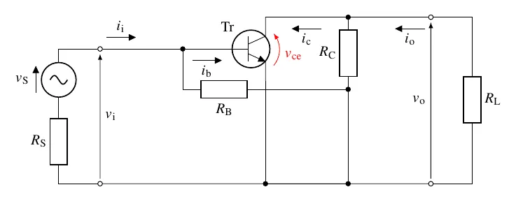
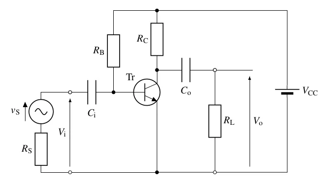
本記事で扱う固定バイアス増幅回路を下図に示します。
- はベース-エミッタ間にバイアス電圧を与え、ベース電流 を制限するための抵抗、 は交流電圧を増幅し、またコレクタ-エミッタ間電圧を設定するための抵抗です(詳細は固定バイアス回路の説明を参照)。
- 、 は結合コンデンサです。結合コンデンサとは、直流成分を遮断し、交流成分のみを伝達させるために、回路の段間に接続するコンデンサです。
- 、 は、入力信号 の起電力と内部抵抗をそれぞれ表しており、信号源の等価回路を構成しています。
- は、出力信号を流す負荷抵抗です。
この回路の動作を簡単に説明すると、ベース電流 の小さな変動でコレクタ電流 を大きく変化させるトランジスタの性質を利用して、 で に比例する電圧降下を生み出して出力端子から取り出す構造となっています。
以下では上図の回路に交流信号 、 が入力されたときの動作を具体的に調べていきます。 ただし、、、 とします。
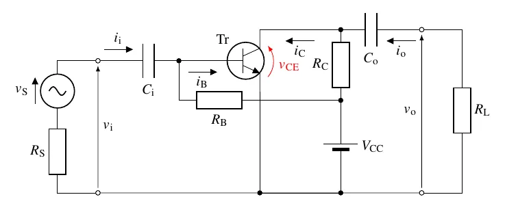
図式解析
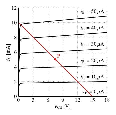
ここでは、トランジスタの出力特性が下図で表されるものとします2。 また、ベース電流の直流成分(バイアス電流)は とします。
出力特性のグラフを用いた交流動作の解析は以下の手順で行います。
- 直流負荷線の作図
- 動作点の作図
- 交流負荷線の作図と読み取り
交流負荷線も直流負荷線と同じ動作点を通るので、交流動作の解析の前に動作点を求める必要があります。
1. 直流負荷線の作図
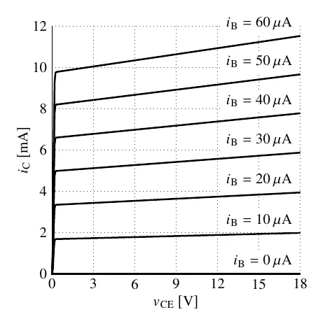
ということで、まずは直流動作を考えます。 直流成分だけ見れば、結合コンデンサ と によって信号源や負荷が分離されています。 したがって、固定バイアス増幅回路は直流成分に対しては前回の記事で扱った下図の固定バイアス回路と等価です(、 はそれぞれ 、 に読み替えてください)。
直流負荷線の式は となります。 また、、 より、負荷線は と の2点を通る直線であることが分かります(下図の赤実線)。
2. 動作点の作図
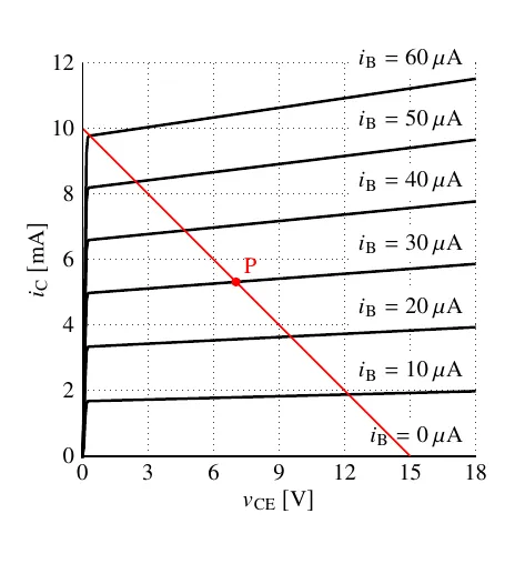
動作点は直流負荷線上に作図します。 バイアス電流 より、動作点は の出力特性曲線と直流負荷線の交点 となります(下図の点P)。
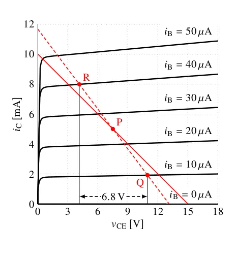
3. 交流負荷線の作図と読み取り
続いて交流動作を考えます。 コンデンサは一般に交流電流を通過させるので、交流動作を考える際は結合コンデンサの端子間を短絡します3。 また、電圧源 は電流の変化によらず常に一定の電圧を供給することから交流的なインピーダンスは零なので、電圧源も短絡とみなせます。 したがって、交流動作はコンデンサと電圧源を短絡した下図の回路で考えます。
交流負荷線は出力特性のグラフ上に作図するので、直流負荷線と同様に出力端子であるコレクタ-エミッタ間から回路を見ると、 と が並列に接続されています。 これを抜き出したのが下図です。
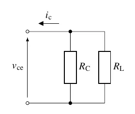
上図について、オームの法則より以下の関係が成立します。
よって、交流負荷線の傾きは以下で表されます。
上式に値を代入すると となります。 これは、 が (グラフでは3目盛分)増加するごとに が (グラフでは4目盛分)減少することを示しています。 以上より、交流負荷線は下図の赤破線で表される直線となります。
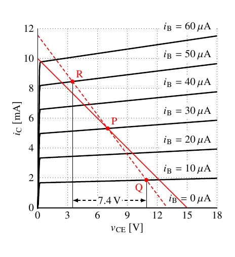
いま、ベース電流の交流成分 の振幅が であるとします。 このとき、コレクタ電流 やコレクタ-エミッタ間電圧 がどのように変化するのかを交流負荷線から読み取ることができます。 はバイアス電流 から 変動することになります。 波形のピークを考えると、 のとき点P にある は、 と の各特性曲線と交流負荷線の交点間(上図のQ-R間)を動くことになります。
上図より、 のピークピーク値は 7.4 V であることが分かります。 振幅はピークピーク値の1/2のため 3.7 V であり、 と は逆相の関係にあります。 波形の歪みを無視すると、ベース電流が のとき、 の両端電圧は で表されます(:角周波数、:時刻)。 同様に電流 については、およそ 2 mA から 8.5 mA の間をピークピーク値 6.5 mA で変化することから、歪みを無視すると で表されます。
ただ、上図をよく見るとPQ間の距離とPR間の距離が等しくありません。 これは前回の記事で述べたアーリー効果によるものです。 仮に の波形が正負対称だとしても、 や の波形は非対称となることが分かります。 このように図式解析では、線形性を仮定する小信号等価回路では読み取ることのできない波形の歪み方まで読み取ることが可能です。 そのため、振幅の大きな信号を扱う電力増幅回路では小信号等価回路ではなく図式解析を用いて動作を調べるそうです。
練習問題1
※ この問題を解くためには作図が必要です
上図のトランジスタ回路におけるトランジスタの出力特性を下図に示す。 ベース電流 が時刻 の関数として で表されるとき、コレクタ-エミッタ間電圧 を時刻 の関数として表せ。 ただし、、、 とし、、 は十分大きいものとする。 また、波形の歪みは無視できるものとする。
解説
直流負荷線、動作点、交流負荷線の順に作図し、 の動作点の値 とピークピーク値を求めます。
- 直流負荷線は上述した と の2点を通る直線となります。
- の直流成分は ですが、 の出力特性曲線はグラフに描画されていません。このため、 と直流負荷線との交点 及び の各曲線と直流負荷線との交点 を1:1で内分する点P を動作点とします。
- 交流負荷線の傾きは上述した です。 動作点を通るように直線を描画すると下図の赤破線のようになります。
題意より であることから、 は上図の交流負荷線上のQ-R間を動きます。 このため のピークピーク値は 6.8 V です。 仮定より波形の歪みを無視すると は次式で表されます。
小信号等価回路
前回の記事で見たように、本来トランジスタの入力特性や出力特性は非線形ですが、それを線形として近似できるほど小さな振幅の信号に対して、増幅度や入力インピーダンス、出力インピーダンスを解析する際に有用なのが小信号等価回路です。 小信号等価回路は動作点近傍のトランジスタの入力特性と出力特性を線形とみなしてでモデル化するものであり、直流動作に対しては適用できないほか、振幅の大きな信号を扱う回路の交流動作に対しては大きな誤差が生じます。
トランジスタの小信号等価回路にはいくつか種類がありますが、本記事では パラメータによる等価回路を利用します。
hパラメータによるトランジスタの等価回路
四端子回路を表すための 行列の一種であるハイブリッド行列の各成分を パラメータ( 定数とも)と呼びます。
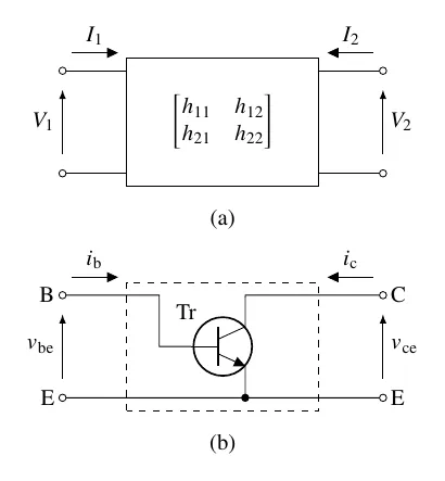
上図(a)のように電圧 、電流 の入力端と電圧 、電流 の出力端を備えた四端子回路を考えます。 この回路の入出力関係は、ハイブリッド行列を用いると以下の式で表現できます。
パラメータは下表に示す4つの物理量の総称です。 上式では添え字に数字を用いて表記しましたが、トランジスタの パラメータを表す際は、電気的な意味が分かりやすい英字の添え字がしばしば利用されます。
| 表記1 | 表記2 | 意味 |
|---|---|---|
| 出力端短絡時の入力インピーダンス | ||
| 入力端開放時の逆方向電圧帰還率 | ||
| 出力端短絡時の順方向電流増幅率 | ||
| 入力端開放時の出力アドミタンス |
トランジスタは3極から成る素子ですが、いずれかを接地するので四端子回路として扱えます。 エミッタ接地の場合は上図(b)のように、ベース-エミッタ間を入力(電圧 、電流 )、コレクタ-エミッタ間を出力(電圧 、電流 )とします。
また、トランジスタの パラメータはどの端子を接地するのかによって値が異なるため、添え字に接地する端子を示す英字を付して表記されます(例:エミッタ接地電流増幅率は )。 したがって、エミッタ接地トランジスタの入出力関係は以下の式で表されます。
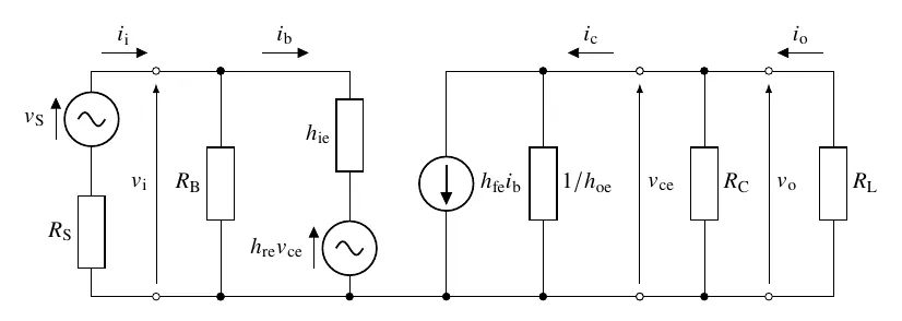
上式を回路図で表すと下図(c)に示す パラメータによる小信号等価回路が得られます。
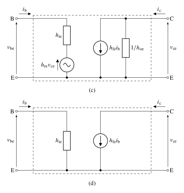
上図(d)はエミッタ接地トランジスタの簡易等価回路です。 簡易等価回路では、値の小さい や を無視し、、 としています。
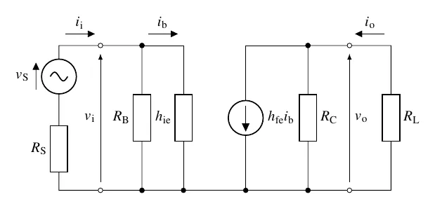
固定バイアス増幅回路の小信号等価回路
固定バイアス増幅回路の交流動作を考えるために、交流負荷線のときと同様にコンデンサと電圧源を短絡した下図の回路を考えます。
この増幅回路のうちトランジスタを図(c)の等価回路に置換すると、下図に示す固定バイアス増幅回路の小信号等価回路が得られます。
以下ではこの等価回路を用いて増幅回路の増幅度や入力・出力の各インピーダンスを計算します。
増幅度の計算
出力と入力の比は増幅度または利得と呼ばれ、増幅回路の主要な性能指標です。
増幅度は回路のどこを入力とするかによって複数定義が存在しますが、本記事ではトランジスタを入力の基準とする場合を 、信号源と接続する回路の入力端を基準とする場合を で表記します。
- 電圧増幅度
- :回路の入力電圧(この回路ではトランジスタの入力電圧に等しい)に対する回路の出力電圧の比
- :信号源の起電力に対する回路の出力電圧の比
- 信号源の内部抵抗 による入力端の電圧降下を考慮する必要
- 電流増幅度
- :トランジスタの入力電流に対する回路の出力電流の比
- :回路の入力電流に対する回路の出力電流の比
- 入力端の電流のうち に分流する分を考慮する必要
- 電力増幅度
- :トランジスタの入力電力に対する負荷抵抗 に供給される電力の比
- :信号源の起電力 から供給される電力に対する負荷抵抗 に供給される電力の比
出力端の電圧 、電流 はそれぞれ以下の式で表されます。
したがって、電流増幅度 は以下の式で求められます。
より、入力端の電圧 は以下となります。
したがって、電圧増幅度 は以下の式で求められます。
電力増幅度 は上で求めた と を用いて以下の式で計算できます。
また、入力電流 は を用いて以下の式で表されます。
詳細
抵抗 を流れる電流は で表されるため、入力電圧 について以下の等式が成り立ちます。
上式を に関する式に変形すると以下のようになります。
ここに上で求めた を代入すると以下の式が得られます。
よって、電流増幅度 は以下の式で求められます。
電流増幅度 と電力増幅度 は回路の入力インピーダンスを用いて計算するため、それを先に計算します。
入出力インピーダンスの計算
固定バイアス増幅回路の等価回路を用いて、回路の交流的な入力インピーダンスと出力インピーダンスを求めます。
入力インピーダンスは、入力端における電圧 と電流 の比によって求められ、次式で表されます。
出力インピーダンスは における です。 より、入力電圧 について以下の式が成り立ちます。
この を とおくと、 と表されます。 行列の入力側の関係式および より、 は を用いて以下の式で表されます。
行列の出力側の関係式から、、 は を用いて以下の式で表されます。
したがって、出力インピーダンス は次式で表されます。
ここで です。
信号源内部抵抗を考慮した増幅度
信号源内部抵抗 を考慮した電圧増幅度 を求めます。 まず入力電圧 は、上で求めた回路の入力インピーダンス と起電力 を用いて以下の式で表されます。
したがって、電圧増幅度 は以下の式で求められます。
電力増幅度 は と を用いて以下の式で計算できます。
増幅度と入出力インピーダンスのまとめ
を以下のようにおきます。
また、ハイブリッド行列の行列式を とおきます。
出力端と入力端それぞれにおける電圧と電流は を用いて以下の式で表されます。
増幅度や入出力インピーダンスは以下となります。
- トランジスタの入力端を基準とする増幅度
- 回路の入力端を基準とする増幅度
- 回路の入力インピーダンス及び出力インピーダンス
練習問題2
下図のトランジスタ回路の電圧増幅度 の大きさを求めよ。 ただし、、 とし、、 は十分大きいものとする。 また、トランジスタの パラメータを下表に示す値とする。
名称 記号 値 入力インピーダンス 電圧帰還率 電流増幅率 出力アドミタンス
解説
上図は本記事で扱っている固定バイアス増幅回路です。 結合コンデンサ 、 によって と は直流成分をもたないので、上で導出した電圧増幅度 の式に値を代入することで の大きさを求めることができます。
練習問題3
下図のトランジスタ回路の電圧増幅度 、電流増幅度 、入力インピーダンス を導出し、それらの値を求めよ。 ただし、、、 とし、、 は十分大きいものとする。 また、トランジスタの パラメータのうち 及び を下表に示す値とし、 及び の影響は無視するものとする。
名称 記号 値 入力インピーダンス 電流増幅率
解説
仮定より なので、トランジスタを図(d)の簡易等価回路で置換すると、下図に示す固定バイアス増幅回路の簡易等価回路が得られます。
この簡易等価回路を用いて増幅回路の電圧増幅度や電流増幅度を計算します。
入力電圧 、出力電圧 はそれぞれ以下の式で表されます。
したがって、電圧増幅度 は以下の式で求められます。
入力電流 、出力電流 はそれぞれ以下の式で表されます。
したがって、電流増幅度 は以下の式で求められます。
入力インピーダンス は と の比であり、次式で表されます。
値を代入します。
※ 回路の出力インピーダンス は を無視すると となります。
簡易等価回路の近似精度
練習問題2・3のパラメータを用いて計算した、、 を考慮する小信号等価回路と考慮しない簡易等価回路の各回路における増幅度と入出力インピーダンス、そしてそれらの誤差率を下表に示します。 ここで、、 の計算にあたっては、信号源内部抵抗を としました。
- 本記事と併せて作成した計算ツールを利用すれば、異なるパラメータに対する計算結果を得ることができます。
| 名称 | 小信号等価回路 | 簡易等価回路 | 誤差率 |
|---|---|---|---|
| 電流増幅度 | 40.24 | 42.50 | 5.62% |
| 電圧増幅度 | -190.9 | -197.2 | 3.26% |
| 電力増幅度 | 7683 | 8380 | 9.07% |
| 電流増幅度 | 40.16 | 42.42 | 5.62% |
| 電圧増幅度 | -181.4 | -187.5 | 3.37% |
| 電力増幅度 | 7283 | 7952 | 9.18% |
| 入力インピーダンス | 2.29% | ||
| 出力インピーダンス | 4.50% |
この表から、練習問題2・3のパラメータにおいては簡易等価回路でも 10% 以内の誤差率で計算できていることが分かります。 実際の回路では部品ごとのばらつきの影響があることを考慮すると(例えば一般的な炭素被膜抵抗の誤差率は 5%)、簡易等価回路で実用上妥当な近似値が得られていると考えられます。
hパラメータ hie について
パラメータのうち は、 と共に簡易等価回路の計算で必要なパラメータです。 数値を入れて計算すると分かるのですが、電圧増幅度 は によって大きく変動します。 また上の表で見られるように、固定バイアス増幅回路においては、入力インピーダンス について の影響が支配的となっています。 この は、前回の記事で扱った入力特性の動作点における傾きの逆数と等しくなります(ちなみに は動作点における出力特性の傾きです)。 ここで、入力特性の理論式であるショックレーの式を用いて の計算式を導出します。
ショックレーの式によれば、ベース電流 はベース・エミッタ間電圧 の関数として、次式で表されます。
ここで、 は逆方向飽和電流であり、 は熱電圧です。熱電圧は物理定数を用いて と定義され、25℃においては となります。なお、 はボルツマン定数、 は絶対温度、 は電気素量を表します。 上式を微分すると次式が得られます。
の影響を無視すると となるため、上式の逆数である は近似的に次式で求められます。
上式より、 は に反比例し、 に比例することが分かります。
2SC1815のデータシート4にはコレクタ電流に対する パラメータの図が掲載されており、コレクタ電流が 6 mA のときのYランクを見ると、、 程度です。 熱電圧を として上式で概算した値は なので、まずまずの値が得られています。
多くのトランジスタのデータシートには も も掲載されていないため、そのような場合は と仮定して上式を計算することにより、 を概算することができます。
結合コンデンサの条件
ここまで結合コンデンサ と の静電容量については、練習問題の問題文に記載したように「十分大きいもの」、つまり交流成分の信号は減衰させないものとして扱ってきましたが、実際どのくらいの値のものを使うべきなのでしょうか。 その計算に使うのが、上で求めた入力インピーダンス及び出力インピーダンスです。
結合コンデンサ と入力インピーダンス(または出力インピーダンス) からなる ハイパスフィルタを考えます。 このフィルタ回路の遮断周波数(カットオフ周波数)は で表されます。 このため、入力信号の最低周波数を とおくと、 の関係が成立すれば入力信号を少ない歪みで通過することができます5。 したがって、結合コンデンサの静電容量 の条件は次式で表されます。
信号の最低周波数に対して遮断周波数に十分な余裕を持たせるためには、例えば として設計するのが簡単です。 その場合、各結合コンデンサの静電容量の条件は 、 となります。 例えば最低周波数 の信号を入力する場合、遮断周波数が となるには 、 であればよいので、 の電解コンデンサを使うことができます。
なお、入力信号の信号源を接続すると、その内部抵抗 も フィルタの抵抗分として加わるため、入力側結合コンデンサ による は低下することになります。 同様に負荷を接続すると、その抵抗 の影響で出力側結合コンデンサ による は低下します。
おわりに
本記事では最も単純なエミッタ接地増幅回路である固定バイアス増幅回路を取り上げ、図式解析や等価回路によってその交流動作を調べました。
図式解析では作図した交流負荷線から出力電圧や電流を読み取り、小信号等価回路では パラメータを用いて増幅度や入出力インピーダンスを定式化しました。 簡易等価回路を用いて計算した場合の誤差率も数値的に確認しました。
直流動作も交流動作も理論を切り口に学び、トランジスタの正しい使い方が少しずつ分かってきた気がしています。
回路図のソースコード
回路図は を用いて で作成しています。 ソースコードは以下のとおりです。
固定バイアス増幅回路 (fixed-bias-amp.tex)
% Common Emitter Amplifier (fixed bias)
\documentclass[border=3mm]{standalone}
\usepackage{tikz}
\usepackage{circuitikz}
\ctikzset{transistors/arrow pos=end}
\usepackage{newtxtext,newtxmath}
\pagecolor{white}
\begin{document}
\begin{tikzpicture}
\draw (0,0) node[npn](Tr) {};
\draw[thick] ($(Tr)-(0.35,0)$) circle [radius=13pt] node[above left=8pt] {Tr};
\draw[red, -latex] (0.2,-0.4) arc[x radius=0.6, y radius=0.6, start angle=320, delta angle=80]
    node[below=15pt,right=4pt] {$v_\mathrm{CE}$};
\draw(Tr.C)
    to[short, f<_=$i_\mathrm{C}$] ++(2,0)
    to[european resistor, l_=$R_\mathrm{C}$] ++(0,-1.75)
    coordinate(tmp0) % below Rc
    to[short] ++(-2,0)
    to[european resistor, l=$R_\mathrm{B}$] ++(-2,0)
    coordinate(tmp1) % left Rb
    to[short] ++(0,0.95) |- (Tr.B)
    node[pos=0.5, circ] (tmp3) {};
\draw(tmp3) to[short, f_=$i_\mathrm{B}$] (Tr.B);
\draw(Tr.E)
    to[short] ++(0,-0.5)
    to[short] ++(0,-2)
    coordinate(tmp2); % below Tr.E
\draw(tmp0)
    to[battery2, l=$V_\mathrm{CC}$, *-] ++(0,-2.3) |- (tmp2);
%%% [BEGIN] I/O %%%
% --- Input ---
\draw(tmp3)
    to[short] ++(-0.5,0) to[C, l=$C_\mathrm{i}$] ++(-0.5,0)
    to[short, -o, f_<=$i_\mathrm{i}$] ++(-1,0) node (inp) {};
\draw(tmp2) to[short, *-o] ++(-4,0) node (inn) {};
\draw[-latex] (inn) -- (inp) node[right,pos=0.5] {$v_\mathrm{i}$};
% --- Output ---
\draw(Tr.C) to[short, -*] ++(2,0)
    to[short] ++(0.5,0) to[C, l_=$C_\mathrm{o}$] ++(0.5,0)
    to[short, f_<=$i_\mathrm{o}$, -o] ++(1,0) node (outp) {};
\draw(tmp2) to[short, -*] ++(2,0)
    to[short, -o] ++(2,0) node (outn) {};
\draw[-latex] (outn) -- (outp) node[left,pos=0.5] {$v_\mathrm{o}$};
%%%  [END]  I/O %%%
%%% [BEGIN] Load & Source %%%
\draw(outp.center) to[short, o-] ++(1,0)
    to[european resistor, l=$R_\mathrm{L}$] ++(0,-4) |- (outn.center)
    node[pos=0.5] {} to[short, -o] (outn.center);
\draw(inp.center) to[short, o-] ++(-1,0)
    to[sV_<=$v_\mathrm{S}$] ++(0,-1.5)
    to[european resistor, l_=$R_\mathrm{S}$] ++(0,-1.5) |- (inn.center)
    node[pos=0.5] {} to[short, -o] (inn.center);
%%%  [END]  Load & Source %%%
\end{tikzpicture}
\end{document}
コンデンサ・電圧源を短絡した回路 (capacitor-dcv-short.tex)
% Common Emitter Amplifier (AC)
\documentclass[border=3mm]{standalone}
\usepackage{tikz}
\usepackage{circuitikz}
\ctikzset{transistors/arrow pos=end}
\usepackage{newtxtext,newtxmath}
\pagecolor{white}
\begin{document}
\begin{tikzpicture}
\draw (0,0) node[npn](Tr) {};
\draw[thick] ($(Tr)-(0.35,0)$) circle [radius=13pt] node[above left=8pt] {Tr};
\draw[red, -latex] (0.2,-0.4) arc[x radius=0.6, y radius=0.6, start angle=320, delta angle=80]
    node[below=15pt,right=4pt] {$v_\mathrm{ce}$};
\draw(Tr.C)
    to[short, f<_=$i_\mathrm{c}$] ++(2,0)
    to[european resistor, l_=$R_\mathrm{C}$] ++(0,-1.75)
    coordinate(tmp0) % below Rc
    to[short] ++(-2,0)
    to[european resistor, l=$R_\mathrm{B}$] ++(-2,0)
    coordinate(tmp1) % left Rb
    to[short] ++(0,0.95) |- (Tr.B)
    node[pos=0.5, circ] (tmp3) {};
\draw(tmp3) to[short, f_=$i_\mathrm{b}$] (Tr.B);
\draw(Tr.E)
    to[short] ++(0,-0.5)
    to[short] ++(0,-2)
    coordinate(tmp2); % below Tr.E
\draw(tmp0)
    to[short, *-] ++(0,-2.3) |- (tmp2); % Vcc
%%% [BEGIN] I/O %%%
% --- Input ---
\draw(tmp3)
    to[short] ++(-0.5,0) to[short] ++(-0.5,0) % Ci
    to[short, -o, f_<=$i_\mathrm{i}$] ++(-1,0) node (inp) {};
\draw(tmp2) to[short, *-o] ++(-4,0) node (inn) {};
\draw[-latex] (inn) -- (inp) node[right,pos=0.5] {$v_\mathrm{i}$};
% --- Output ---
\draw(Tr.C) to[short, -*] ++(2,0)
    to[short] ++(0.5,0) to[short] ++(0.5,0) % Co
    to[short, f_<=$i_\mathrm{o}$, -o] ++(1,0) node (outp) {};
\draw(tmp2) to[short, -*] ++(2,0)
    to[short, -o] ++(2,0) node (outn) {};
\draw[-latex] (outn) -- (outp) node[left,pos=0.5] {$v_\mathrm{o}$};
%%%  [END]  I/O %%%
%%% [BEGIN] Load & Source %%%
\draw(outp.center) to[short, o-] ++(1,0)
    to[european resistor, l=$R_\mathrm{L}$] ++(0,-4) |- (outn.center)
    node[pos=0.5] {} to[short, -o] (outn.center);
\draw(inp.center) to[short, o-] ++(-1,0)
    to[sV_<=$v_\mathrm{S}$] ++(0,-1.5)
    to[european resistor, l_=$R_\mathrm{S}$] ++(0,-1.5) |- (inn.center)
    node[pos=0.5] {} to[short, -o] (inn.center);
%%%  [END]  Load & Source %%%
\end{tikzpicture}
\end{document}
出力部分を抽出した回路 (ac-load.tex)
% Common Emitter Amplifier (AC load)
\documentclass[border=3mm]{standalone}
\usepackage{tikz}
\usepackage{circuitikz}
\usepackage{newtxtext,newtxmath}
\pagecolor{white}
\begin{document}
\begin{tikzpicture}
\draw (0,0)
    to[short, o-, f<=$i_\mathrm{c}$] ++(1.5,0)
    to[european resistor, l=$R_\mathrm{C}$] ++(0,-2.5)
    to[short, -o] ++(-1.5,0);
\draw (1.5,0)
    to[short, *-] ++(1.2,0)
    to[european resistor, l=$R_\mathrm{L}$] ++(0,-2.5)
    to[short, -*] ++(-1.2,0);
\draw[latex-] (0,-0.2) -- (0,-2.3) node[left,pos=0.5] {$v_\mathrm{ce}$};
\end{tikzpicture}
\end{document}
hパラメータによる等価回路表現 (1) (h-param-circuit-1.tex)
% h Parameters for Common Emitter BJT
\documentclass[border=3mm]{standalone}
\usepackage{tikz}
\usepackage{circuitikz}
\ctikzset{transistors/arrow pos=end}
\usepackage{newtxtext,newtxmath}
\pagecolor{white}
\begin{document}
\begin{tikzpicture}
\begin{scope}
    \draw (-1.5,-1) rectangle (1.5,1);
    \node (0,0) {$\begin{bmatrix}
       h_{11} & h_{12} \\
       h_{21} & h_{22}
    \end{bmatrix}$};
    \draw (-1.5, 0.8) to[short, -o, f<_=$I_1$] ++(-1,0);
    \draw (-1.5,-0.8) to[short, -o] ++(-1,0);
    \draw ( 1.5, 0.8) to[short, -o, f<=$I_2$] ++(1,0);
    \draw ( 1.5,-0.8) to[short, -o] ++(1,0);
    \draw[-latex] (-2.5,-0.5) -- (-2.5,0.5) node[pos=0.5, left] {$V_1$};
    \draw[-latex] ( 2.5,-0.5) -- ( 2.5,0.5) node[pos=0.5, right] {$V_2$};
    \node[below] at (0,-1.25) {(a)};
\end{scope}
\begin{scope}[yshift=-3.5cm]
    \draw (0.35,0) node[npn](Tr) {};
    \draw[thick] ($(Tr)-(0.35,0)$) circle [radius=13pt] node[above left=8pt] {Tr};
    \draw (Tr.B) to[short] ++(-0.5,0) to[short] ++(0,0.8)
        to[short] (-1.5,0.8) to[short, -o, f<_=$i_\mathrm{b}$] (-2.5,0.8)
        node[left] {B};
    \draw (Tr.C) to[short] ++(0,0.01) |- (2.5,0.8)
        node[pos=0.5] {} to[short] (1.5,0.8) to[short, -o, f<=$i_\mathrm{c}$] (2.5,0.8)
        node[right] {C};
    \draw (Tr.E) to[short, -*] ++(0,-0.03) |- (2.5,-0.8)
        node[pos=0.5] {} to[short, -o] (-2.5,-0.8) node[left] {E}
        node[pos=0.5] {} to[short, -o] (2.5,-0.8) node[right] {E};
    \draw[-latex] (-2.5,-0.5) -- (-2.5,0.5) node[pos=0.5, left] {$v_\mathrm{be}$};
    \draw[-latex] ( 2.5,-0.5) -- ( 2.5,0.5) node[pos=0.5, right] {$v_\mathrm{ce}$};
    \draw[dashed] (-1.5,-1) rectangle (1.5,1);
    \node[below] at (0,-1.25) {(b)};
\end{scope}
\end{tikzpicture}
\end{document}
hパラメータによる等価回路表現 (2) (h-param-circuit-2.tex)
% Equivalent Circuit of Common Emitter BJT
\documentclass[border=3mm]{standalone}
\usepackage{tikz}
\usepackage{circuitikz}
\usepackage{newtxtext,newtxmath}
\pagecolor{white}
\begin{document}
\begin{tikzpicture}
\begin{scope}
    \draw (0,0) to[european resistor, l_=$h_\mathrm{ie}$] ++(0,-2)
        to[sV_<=$h_\mathrm{re}v_\mathrm{ce}$, -*] ++(0,-1.5);
    \draw (2,0) to[american current source, l=$h_\mathrm{fe}i_\mathrm{b}$, -*] ++(0,-3.5);
    \draw (2,0) to[short, -*] ++(1.5,0)
        to[european resistor, l=$1/h_\mathrm{oe}$, -*] ++(0,-3.5);
    \draw (0,0) to[short] ++(-2,0) to[short, f<_=$i_\mathrm{b}$, -o] ++(-1,0) node[left] {B};
    \draw (2,0) to[short] ++( 3,0) to[short, f<=$i_\mathrm{c}$, -o] ++(1,0) node[right] {C};
    \draw (-3,-3.5) node[left] {E} to[short, o-o] ++(9,0) node[right] {E};
    \draw[-latex] (-3,-3.3) -- (-3,-0.2) node[pos=0.5, left] {$v_\mathrm{be}$};
    \draw[-latex] ( 6,-3.3) -- ( 6,-0.2) node[pos=0.5, right] {$v_\mathrm{ce}$};
    \draw[dashed] (-2,0.2) rectangle (5,-3.7);
    \node[below] at (1.5,-4) {(c)};
\end{scope}
\begin{scope}[yshift=-5.5cm]
    \draw (0,0) to[european resistor, l_=$h_\mathrm{ie}$, -*] ++(0,-3.5);
    \draw (2,0) to[american current source, l=$h_\mathrm{fe}i_\mathrm{b}$, -*] ++(0,-3.5);
    \draw (0,0) to[short] ++(-2,0) to[short, f<_=$i_\mathrm{b}$, -o] ++(-1,0) node[left] {B};
    \draw (2,0) to[short] ++( 3,0) to[short, f<=$i_\mathrm{c}$, -o] ++(1,0) node[right] {C};
    \draw (-3,-3.5) node[left] {E} to[short, o-o] ++(9,0) node[right] {E};
    \draw[-latex] (-3,-3.3) -- (-3,-0.2) node[pos=0.5, left] {$v_\mathrm{be}$};
    \draw[-latex] ( 6,-3.3) -- ( 6,-0.2) node[pos=0.5, right] {$v_\mathrm{ce}$};
    \draw[dashed] (-2,0.2) rectangle (5,-3.7);
    \node[below] at (1.5,-4) {(d)};
\end{scope}
\end{tikzpicture}
\end{document}
固定バイアス増幅回路の等価回路 (amp-equiv-circuit.tex)
% Equivalent Circuit of Common Emitter Amplifier (w/ hre, hoe)
\documentclass[border=3mm]{standalone}
\usepackage{tikz}
\usepackage{circuitikz}
\usepackage{newtxtext,newtxmath}
\pagecolor{white}
\begin{document}
\begin{tikzpicture}
%%% [BEGIN] equivalent circuit of common emitter BJT %%%
\draw (0,0) to[european resistor, l_=$h_\mathrm{ie}$] ++(0,-2)
    to[sV_<=$h_\mathrm{re}v_\mathrm{ce}$, -*] ++(0,-1.5);
\draw (1.5,0) to[american current source, l=$h_\mathrm{fe}i_\mathrm{b}$, -*] ++(0,-3.5);
\draw (1.5,0) to[short, -*] ++(1.5,0)
    to[european resistor, l=$1/h_\mathrm{oe}$, -*] ++(0,-3.5);
\draw (0,0) to[short, f<_=$i_\mathrm{b}$, -o] ++(-2,0);
\draw (3,0) to[short, f<=$i_\mathrm{c}$, -o] ++(1.5,0);
\draw (-2,-3.5) to[short, o-o] (4.5,-3.5);
\draw[-latex] (4.5,-3.3) -- (4.5,-0.2) node[pos=0.5, right] {$v_\mathrm{ce}$};
%%%  [END]  equivalent circuit of common emitter BJT %%%
%%% [BEGIN] input %%%
\draw (-2,0) to[european resistor, l_=$R_\mathrm{B}$, *-*] ++(0,-3.5);
\draw (-2,0) to[short, -o] ++(-1,0) to[short, f<_=$i_\mathrm{i}$] ++(-1,0)
    to[sV_<=$v_\mathrm{S}$] ++(0,-1.5)
    to[european resistor, l_=$R_\mathrm{S}$] ++(0,-2)
    to[short] ++(1,0) to[short, o-] ++(1,0);
\draw[-latex] (-3,-3.3) -- (-3,-0.2) node[pos=0.5, left] {$v_\mathrm{i}$};
%%%  [END]  input %%%
%%% [BEGIN] output %%%
\draw (4.5,0) to[short, o-*] ++(1,0)
    to[european resistor, l=$R_\mathrm{C}$] ++(0,-3.5) to[short, *-o] ++(-1,0);
\draw (5.5,0) to[short, -o] ++(1,0) to[short, f<=$i_\mathrm{o}$] ++(1,0)
    to[european resistor, l=$R_\mathrm{L}$] ++(0,-3.5) to[short] ++(-1,0)
    to[short, o-] ++(-1,0);
\draw[-latex] (6.5,-3.3) -- (6.5,-0.2) node[pos=0.5, right] {$v_\mathrm{o}$};
%%%  [END]  output %%%
\end{tikzpicture}
\end{document}
固定バイアス増幅回路の簡易等価回路 (amp-simple-equiv-circuit.tex)
% Equivalent Circuit of Common Emitter Amplifier (w/o hre, hoe)
\documentclass[border=3mm]{standalone}
\usepackage{tikz}
\usepackage{circuitikz}
\usepackage{newtxtext,newtxmath}
\pagecolor{white}
\begin{document}
\begin{tikzpicture}
%%% [BEGIN] equivalent circuit of common emitter BJT %%%
\draw (0,0) to[european resistor, l_=$h_\mathrm{ie}$, -*] ++(0,-3.5);
\draw (1.5,0) to[american current source, l=$h_\mathrm{fe}i_\mathrm{b}$, -*] ++(0,-3.5);
\draw (0,0) to[short, f<_=$i_\mathrm{b}$, -o] ++(-1,0);
\draw (1.5,0) to[short, -o] ++(1.5,0);
\draw (-1,-3.5) to[short, o-o] (3,-3.5);
%%%  [END]  equivalent circuit of common emitter BJT %%%
%%% [BEGIN] input %%%
\draw (-1,0) to[european resistor, l_=$R_\mathrm{B}$, *-*] ++(0,-3.5);
\draw (-1,0) to[short, -o] ++(-1,0) to[short, f<_=$i_\mathrm{i}$] ++(-1,0)
    to[sV_<=$v_\mathrm{S}$] ++(0,-1.5)
    to[european resistor, l_=$R_\mathrm{S}$] ++(0,-2)
    to[short] ++(1,0) to[short, o-] ++(1,0);
\draw[-latex] (-2,-3.3) -- (-2,-0.2) node[pos=0.5, left] {$v_\mathrm{i}$};
%%%  [END]  input %%%
%%% [BEGIN] output %%%
\draw (3,0) to[european resistor, l=$R_\mathrm{C}$, *-*] ++(0,-3.5);
\draw (3,0) to[short, -o] ++(1,0) to[short, f<=$i_\mathrm{o}$] ++(1,0)
    to[european resistor, l=$R_\mathrm{L}$] ++(0,-3.5) to[short] ++(-1,0)
    to[short, o-] ++(-1,0);
\draw[-latex] (4,-3.3) -- (4,-0.2) node[pos=0.5, right] {$v_\mathrm{o}$};
%%%  [END]  output %%%
\end{tikzpicture}
\end{document}
固定バイアス増幅回路(練習問題) (practice-fixed-bias-amp.tex)
% Common Emitter Amplifier (fixed bias)
\documentclass[border=3mm]{standalone}
\usepackage{tikz}
\usepackage{circuitikz}
\usetikzlibrary{calc}
\ctikzset{transistors/arrow pos=end}
\usepackage{newtxtext,newtxmath}
\pagecolor{white}
\begin{document}
\begin{tikzpicture}
\draw (0,0) node[npn](Tr) {};
\draw[thick] ($(Tr)-(0.35,0)$) circle [radius=13pt] node[above left=8pt] {Tr};
\draw(Tr.E)
    to[short, -*] ++(0,-2)
    coordinate(tmp3) % below Re
    to[short] ++(2,0)
    coordinate(tmp6) % below Rl
    to[short] ++(2.5,0)
    to[battery2, invert, l_=$V_\mathrm{CC}$] ++(0,5.6)
    to[short] ++(-4.5,0)
    coordinate(tmp1) % above Rc
    to[european resistor, l_=$R_\mathrm{C}$] ++(0,-2)
    to[short] (Tr.C);
\draw(tmp1)
    to[short, *-] ++(-1.5,0)
    to[european resistor, l_=$R_\mathrm{B}$] ++(0,-2.8) |- (Tr.B)
    node[pos=0.5, coordinate] (tmp5) {};
\draw(tmp5) to[short, *-] (Tr.B);
\draw(Tr.C)
    to[C, l_=$C_\mathrm{o}$, *-] ++(2,0)
    coordinate(tmp7)
    to[european resistor, l=$R_\mathrm{L}$, o-o] (tmp6);
\draw(tmp5)
    to[C, l=$C_\mathrm{i}$, -o] ++(-1.5,0)
    coordinate(tmp8);
\draw(tmp3)
    to[short] ++(-3,0)
    coordinate(tmp9)
    to[short, o-] ++(-1,0)
    to[european resistor, l=$R_\mathrm{S}$] ++(0,1.6)
    to[sV=$v_\mathrm{S}$] ++(0,1) |- (tmp8) to[short, -o] (tmp8);
\draw(tmp7) to[short, o-] ++(1.3,0);
\draw[-latex] ($(tmp6)+(1.2,0.2)$) -- ($(tmp7)+(1.2,-0.2)$)
    node[pos=0.5, right] {$V_\mathrm{o}$};
\draw[-latex] ($(tmp9)+(0,0.2)$) -- ($(tmp8)+(0,-0.2)$)
    node[pos=0.5, left] {$V_\mathrm{i}$};
\end{tikzpicture}
\end{document}
その他図面のソースコード
回路図以外の図も を用いて で作成しています。 ソースコードは以下のとおりです。
交流負荷線の説明図 (ac-load-line.tex)
% Output Characteristics Curve (w/ AC load line)
\documentclass[border=3mm]{standalone}
\usepackage{tikz}
\usetikzlibrary{intersections,calc}
\usepackage{newtxtext,newtxmath}
\pagecolor{white}
\begin{document}
\begin{tikzpicture}
\draw[darkgray,dotted] (6,6) grid (0,0);
% .model 2SC1815 NPN (IS=4E-14 BF=170 BR=3.6 VA=100 IK=0.25 RB=50 RC=0.76
% + CJC=4.8p CJE=12p TF=0.63n TR=25n)
%%% [BEGIN] Characteristics (sketch) %%%
\draw[very thick] (0,0) -- +(6,0)
    node[above left,fill=white] {$i_\mathrm{B}=0\mathrm{\,\mu A}\,$};
\draw [very thick,name path=c1] (0,-0.005) -- (0.02,0.13) -- (0.04,0.565) -- (0.06,0.802) -- (0.08,0.837) -- (0.1,0.841) -- (6,0.991)
    node[above left,fill=white] {$i_\mathrm{B}=10\mathrm{\,\mu A}\,$};
\draw [very thick,name path=c2] (0,-0.01) -- (0.02,0.258) -- (0.04,1.112) -- (0.06,1.59) -- (0.08,1.662) -- (0.1,1.671) -- (6,1.968)
    node[above left,fill=white] {$i_\mathrm{B}=20\mathrm{\,\mu A}\,$};
\draw [very thick,name path=c3] (0,-0.015) -- (0.02,0.383) -- (0.04,1.643) -- (0.06,2.365) -- (0.08,2.477) -- (0.1,2.49) -- (6,2.933)
    node[above left,fill=white] {$i_\mathrm{B}=30\mathrm{\,\mu A}\,$};
\draw [very thick,name path=c4] (0,-0.02) -- (0.02,0.506) -- (0.04,2.158) -- (0.06,3.127) -- (0.08,3.28) -- (0.1,3.298) -- (6,3.886)
    node[above left,fill=white] {$i_\mathrm{B}=40\mathrm{\,\mu A}\,$};
\draw [very thick,name path=c5] (0,-0.024) -- (0.02,0.628) -- (0.04,2.659) -- (0.06,3.876) -- (0.08,4.074) -- (0.1,4.097) -- (6,4.827)
    node[above left,fill=white] {$i_\mathrm{B}=50\mathrm{\,\mu A}\,$};
\draw [very thick,name path=c6] (0,-0.029) -- (0.02,0.747) -- (0.04,3.145) -- (0.06,4.613) -- (0.08,4.857) -- (0.1,4.886) -- (6,5.757)
    node[above left,fill=white] {$i_\mathrm{B}=60\mathrm{\,\mu A}\,$};
%%%  [END]  Characteristics (sketch) %%%
%%% [BEGIN] Load line and operating point %%%
\draw[thick,red,name path=loadDC] (5,0) -- (0,5);
\fill[name intersections={of=c3 and loadDC, name=p}];
\fill[red] (p-1) circle[radius=2pt] node[above right,red] {P};
\path[name path=loadAC] (p-1) ++(-3,4) -- ++(6,-8);
\path[name path=ll] (0,0) -- (0,6);
\path[name path=lb] (0,0) -- (6,0);
\path[name intersections={of=loadAC and ll, name=pll}];
\path[name intersections={of=loadAC and lb, name=plb}];
\draw[densely dashed,thick,red] (pll-1) -- (plb-1);
%%  [END]  Load line and operating point %%%
%%% [BEGIN] Extension line and dimension line %%%
\fill[name intersections={of=c5 and loadAC, name=p5}];
\fill[name intersections={of=c1 and loadAC, name=p1}];
\draw (p5-1) -- ($(0,0)!(p5-1)!(6,0)$);
\draw (p1-1) -- ($(0,0)!(p1-1)!(6,0)$);
\draw[thick,densely dashed,latex-latex] ($(0,0.25)!(p5-1)!(6,0.25)$) -- ($(0,0.25)!(p1-1)!(6,0.25)$)
    node[pos=0.5, fill=white, inner sep=1pt] {$7.4\mathrm{\,V}$};
\fill[red] (p1-1) circle[radius=2pt] node[below left,red] {Q};
\fill[red] (p5-1) circle[radius=2pt] node[above right,red] {R};
%%%  [END]  Extension line and dimension line %%%
%%% [BEGIN] Axes %%%
\draw (0,0) -- (6,0) (0,0) -- (0,6);
\foreach \i in {0,1,...,6} \node[below] at (\i,0) {\the\numexpr\i*3\relax};
\foreach \i in {0,1,...,6} \node[left]  at (0,\i) {\the\numexpr\i*2\relax};
\node[below] at (3,-0.4) {$v_\mathrm{CE}\mathrm{\,[V]}$};
\node[rotate=90,above] at (-0.4,3) {$i_\mathrm{C}\mathrm{\,[mA]}$};
%%%  [END]  Axes %%%
\end{tikzpicture}
\end{document}
練習問題1の解答 (practice-ac-load-line.tex)
% Output Characteristics Curve (w/ AC load line)
\documentclass[border=3mm]{standalone}
\usepackage{tikz}
\usetikzlibrary{intersections,calc}
\usepackage{newtxtext,newtxmath}
\pagecolor{white}
\begin{document}
\begin{tikzpicture}
\draw[darkgray,dotted] (6,6) grid (0,0);
%%% [BEGIN] Characteristics (sketch) %%%
\def\offset{-0.45}
\def\theta{89} % deg
\def\alpha{1.05} % deg
\def\beta{1}
\path[name path=lr] (6,0) -- (6,6);
\foreach \i in {1,...,5} {
    \edef\curvepath{(\theta:{\offset+\i/sin(\theta)*\beta^\i}) .. controls +(80:0.35) .. ++({\alpha*\i+35}:0.6)}
    \path[name path=c\i] (0,0) -- \curvepath -- +({\alpha*\i}:5.6);
    \path[name intersections={of=lr and c\i, name=p}];
    \draw[very thick] (0,0) -- \curvepath -- (p-1)
        node[above left,fill=white] {$i_\mathrm{B}=\the\numexpr\i*10\relax\mathrm{\,\mu A}\,$};
}
    \draw[very thick] (0,0) -- +(6,0)
        node[above left,fill=white] {$i_\mathrm{B}=0\mathrm{\,\mu A}\,$};
%%%  [END]  Characteristics (sketch) %%%
%%% [BEGIN] Load line and operating point %%%
\draw[thick,red,name path=loadDC] (5,0) -- (0,5);
\fill[name intersections={of=c3 and loadDC, name=p3}];
\fill[name intersections={of=c2 and loadDC, name=p2}];
\path ($(p3-1)!.5!(p2-1)$) coordinate (p-1);
\fill[red] (p-1) circle[radius=2pt] node[above right,red] {P};
\path[name path=loadAC] (p-1) ++(-3,4) -- ++(6,-8);
\path[name path=ll] (0,0) -- (0,6);
\path[name path=lb] (0,0) -- (6,0);
\path[name intersections={of=loadAC and ll, name=pll}];
\path[name intersections={of=loadAC and lb, name=plb}];
\draw[densely dashed,thick,red] (pll-1) -- (plb-1);
%%  [END]  Load line and operating point %%%
%%% [BEGIN] Extension line and dimension line %%%
\fill[name intersections={of=c4 and loadAC, name=p4}];
\fill[name intersections={of=c1 and loadAC, name=p1}];
\draw (p4-1) -- ($(0,0)!(p4-1)!(6,0)$);
\draw (p1-1) -- ($(0,0)!(p1-1)!(6,0)$);
\draw[thick,densely dashed,latex-latex] ($(0,0.25)!(p4-1)!(6,0.25)$) -- ($(0,0.25)!(p1-1)!(6,0.25)$)
    node[pos=0.5, fill=white, inner sep=1pt] {$6.8\mathrm{\,V}$};
\fill[red] (p1-1) circle[radius=2pt] node[below left,red] {Q};
\fill[red] (p4-1) circle[radius=2pt] node[above right,red] {R};
%%%  [END]  Extension line and dimension line %%%
%%% [BEGIN] Axes %%%
\draw (0,0) -- (6,0) (0,0) -- (0,6);
\foreach \i in {0,1,...,6} \node[below] at (\i,0) {\the\numexpr\i*3\relax};
\foreach \i in {0,1,...,6} \node[left]  at (0,\i) {\the\numexpr\i*2\relax};
\node[below] at (3,-0.4) {$v_\mathrm{CE}\mathrm{\,[V]}$};
\node[rotate=90,above] at (-0.4,3) {$i_\mathrm{C}\mathrm{\,[mA]}$};
%%%  [END]  Axes %%%
\end{tikzpicture}
\end{document}
脚注
-
直流成分については、後述する結合コンデンサの働きでトランジスタ回路の直流動作(動作点の設定)や交流動作(交流信号の増幅)に影響を及ぼさないことから、本記事では交流成分のみを考慮します。 ↩ ↩2
-
pnp型トランジスタ2SC1815の回路シミュレータSPICE用のシミュレーションモデルを利用して取得した出力特性です。モデルは次のリンク先ページに記載のものを使用しています。LTspice ガイド 電気電子回路演習編、京都大学OCW、2019年3月29日 ↩
-
結合コンデンサ 、 の端子間を短絡とみなせる周波数の交流信号が流れていることが前提条件となります。 ↩
-
2SC1815 和文データシート、東芝セミコンダクター社、2009年7月11日時点のアーカイブ ↩
-
遮断周波数の定義より、 で結合コンデンサを設計した場合、入力信号の低域の信号振幅が最大 減衰し、信号に歪みが生じます。 ↩